当前位置:
X-MOL 学术
›
J. Phys. Chem. C
›
论文详情
Our official English website, www.x-mol.net, welcomes your
feedback! (Note: you will need to create a separate account there.)
Formation of Near-IR Excitons in Low-Dimensional CuSbS2
The Journal of Physical Chemistry C ( IF 3.3 ) Pub Date : 2021-09-20 , DOI: 10.1021/acs.jpcc.1c06530 Kevin M. Conley 1 , Caterina Cocchi 2, 3 , Tapio Ala-Nissila 4, 5
The Journal of Physical Chemistry C ( IF 3.3 ) Pub Date : 2021-09-20 , DOI: 10.1021/acs.jpcc.1c06530 Kevin M. Conley 1 , Caterina Cocchi 2, 3 , Tapio Ala-Nissila 4, 5
Affiliation
|
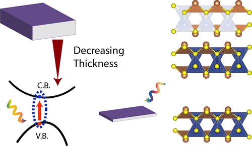
The electronic and optical properties of low-dimensional semiconductors are typically quite different from those of their bulk counterparts. Yet, the optical gap of two-dimensional copper antimony disulfide (CuSbS2) does not dramatically change with decreasing thickness of the material. The absorption onset remains at about 1.5 eV in the monolayer, bilayer, and bulk materials. Using density functional theory and many-body perturbation theory, we rationalize this behavior through the interplay of quantum confinement, electron–hole interactions, and the formation of surface states. Specifically, the spatial confinement in thin layers induces strongly bound optical transitions in the near-infrared region. Our results explain the optical properties in copper antimony disulfide platelets of varying thickness and set these materials as potential candidates for novel photovoltaic devices and near-infrared sensors.
中文翻译:

低维 CuSbS2 中近红外激子的形成
低维半导体的电子和光学特性通常与它们的大块半导体完全不同。然而,二维铜锑二硫化物(CuSbS 2) 不会随着材料厚度的减小而发生显着变化。在单层、双层和块状材料中,吸收起始保持在大约 1.5 eV。使用密度泛函理论和多体微扰理论,我们通过量子限制、电子-空穴相互作用和表面态形成的相互作用使这种行为合理化。具体而言,薄层中的空间限制会在近红外区域引起强束缚的光学跃迁。我们的结果解释了不同厚度的二硫化锑铜片的光学特性,并将这些材料设置为新型光伏器件和近红外传感器的潜在候选材料。
更新日期:2021-09-30
中文翻译:
低维 CuSbS2 中近红外激子的形成
低维半导体的电子和光学特性通常与它们的大块半导体完全不同。然而,二维铜锑二硫化物(CuSbS 2) 不会随着材料厚度的减小而发生显着变化。在单层、双层和块状材料中,吸收起始保持在大约 1.5 eV。使用密度泛函理论和多体微扰理论,我们通过量子限制、电子-空穴相互作用和表面态形成的相互作用使这种行为合理化。具体而言,薄层中的空间限制会在近红外区域引起强束缚的光学跃迁。我们的结果解释了不同厚度的二硫化锑铜片的光学特性,并将这些材料设置为新型光伏器件和近红外传感器的潜在候选材料。


 京公网安备 11010802027423号