当前位置:
X-MOL 学术
›
ACS Appl. Energy Mater.
›
论文详情
Our official English website, www.x-mol.net, welcomes your
feedback! (Note: you will need to create a separate account there.)
Realization of Micropatterned, Narrow Line-Width Ni–Cu–Sn Front Contact Grid Pattern Using Maskless Direct-Write Lithography for Industrial Silicon Solar Cells
ACS Applied Energy Materials ( IF 5.4 ) Pub Date : 2021-09-17 , DOI: 10.1021/acsaem.1c01699 Mahaboobbatcha Aleem 1 , Ramakirshnan Vishnuraj 1 , Balachander Krishnan 1 , Biji Pullithadathil 1
ACS Applied Energy Materials ( IF 5.4 ) Pub Date : 2021-09-17 , DOI: 10.1021/acsaem.1c01699 Mahaboobbatcha Aleem 1 , Ramakirshnan Vishnuraj 1 , Balachander Krishnan 1 , Biji Pullithadathil 1
Affiliation
|
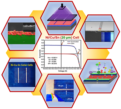
An industry-ready strategic process for the fabrication of cost-effective, micropatterned Ni–Cu–Sn front contact metallization has been demonstrated using maskless direct-write lithography, which could effectively reduce the shadow loss and thereby enhance the efficiency of silicon solar cells by increasing the active area. This investigation also addresses the challenging issues in Ni–Cu–Sn metallization, such as adhesion of the seed layer, low-ohmic contact formation, background plating, and cell processing complications. An eco-friendly aluminum paste with a sheet resistivity of 35 mΩ/cm2 has been developed to fabricate the rear contact on silicon solar cells. A front contact metallization grid with an optimal narrow finger width of 20 μm with an interfinger spacing of 1000 μm has been micropatterned using maskless direct-write lithography for the metallization process. To improve the electrical and mechanical properties of the nickel seed layer, the thickness was optimized as ∼100 nm with a contact resistivity of 6.87 μΩ cm2, which exhibited an adhesion strength of 2.5 N/mm. A low ohmic contact intermediate silicide layer has been created at the Ni–Si interface by the rapid thermal annealing process at 420 °C for 90 s with subsequent copper and tin electroplating to form the Ni–Cu–Sn contacts. An average cell efficiency of 18.5% is achieved for silicon solar cells with a micropatterned Ni–Cu–Sn-based narrow line-width front contact grid design, which could exhibit an ∼1% cell efficiency enhancement as compared to commercial Ag screen-printed solar cells. An ∼6% improvement in cell performance is achieved by reducing the shadow loss with the Ni–Cu–Sn-based front contact metallization as compared to the commercial Ag screen-printed metallization.
中文翻译:

使用无掩模直写光刻技术为工业硅太阳能电池实现微图案化、窄线宽 Ni-Cu-Sn 前接触网格图案
已经使用无掩模直写光刻证明了一种用于制造具有成本效益的微图案化 Ni-Cu-Sn 前接触金属化的工业级战略工艺,该工艺可以有效地减少阴影损失,从而提高硅太阳能电池的效率增加活动面积。这项研究还解决了 Ni-Cu-Sn 金属化中的挑战性问题,例如种子层的粘附、低欧姆接触的形成、背景电镀和电池加工的复杂性。表面电阻率为 35 mΩ/cm 2的环保铝浆已开发用于制造硅太阳能电池上的背面触点。前接触金属化网格的最佳窄指宽度为 20 μm,指间间距为 1000 μm,已使用无掩模直写光刻技术对金属化工艺进行微图案化。为了改善镍种子层的电气和机械性能,将厚度优化为 100 nm,接触电阻率为 6.87 μΩ cm 2,其粘合强度为 2.5 N/mm。通过在 420 °C 下进行 90 秒的快速热退火工艺,在 Ni-Si 界面处形成了低欧姆接触中间硅化物层,随后电镀铜和锡以形成 Ni-Cu-Sn 接触。具有微图案化 Ni-Cu-Sn 基窄线宽前接触网格设计的硅太阳能电池的平均电池效率达到 18.5%,与商业银丝网印刷相比,其电池效率可提高约 1%太阳能电池。与商业银丝网印刷金属化相比,通过减少基于 Ni-Cu-Sn 的前接触金属化的阴影损失,电池性能提高了约 6%。
更新日期:2021-10-25
中文翻译:
使用无掩模直写光刻技术为工业硅太阳能电池实现微图案化、窄线宽 Ni-Cu-Sn 前接触网格图案
已经使用无掩模直写光刻证明了一种用于制造具有成本效益的微图案化 Ni-Cu-Sn 前接触金属化的工业级战略工艺,该工艺可以有效地减少阴影损失,从而提高硅太阳能电池的效率增加活动面积。这项研究还解决了 Ni-Cu-Sn 金属化中的挑战性问题,例如种子层的粘附、低欧姆接触的形成、背景电镀和电池加工的复杂性。表面电阻率为 35 mΩ/cm 2的环保铝浆已开发用于制造硅太阳能电池上的背面触点。前接触金属化网格的最佳窄指宽度为 20 μm,指间间距为 1000 μm,已使用无掩模直写光刻技术对金属化工艺进行微图案化。为了改善镍种子层的电气和机械性能,将厚度优化为 100 nm,接触电阻率为 6.87 μΩ cm 2,其粘合强度为 2.5 N/mm。通过在 420 °C 下进行 90 秒的快速热退火工艺,在 Ni-Si 界面处形成了低欧姆接触中间硅化物层,随后电镀铜和锡以形成 Ni-Cu-Sn 接触。具有微图案化 Ni-Cu-Sn 基窄线宽前接触网格设计的硅太阳能电池的平均电池效率达到 18.5%,与商业银丝网印刷相比,其电池效率可提高约 1%太阳能电池。与商业银丝网印刷金属化相比,通过减少基于 Ni-Cu-Sn 的前接触金属化的阴影损失,电池性能提高了约 6%。


 京公网安备 11010802027423号