Our official English website, www.x-mol.net, welcomes your
feedback! (Note: you will need to create a separate account there.)
In-plane ferroelectricity in few-layered GeS and its van der Waals ferroelectric diodes
Nanoscale ( IF 5.8 ) Pub Date : 2021-08-18 , DOI: 10.1039/d1nr03807a Yong Yan 1 , Qunrui Deng 1 , Shasha Li 1 , Tao Guo 2 , Xueping Li 1 , Yurong Jiang 1 , Xiaohui Song 1 , Wen Huang 3 , Juehan Yang 4 , Congxin Xia 1
Nanoscale ( IF 5.8 ) Pub Date : 2021-08-18 , DOI: 10.1039/d1nr03807a Yong Yan 1 , Qunrui Deng 1 , Shasha Li 1 , Tao Guo 2 , Xueping Li 1 , Yurong Jiang 1 , Xiaohui Song 1 , Wen Huang 3 , Juehan Yang 4 , Congxin Xia 1
Affiliation
|
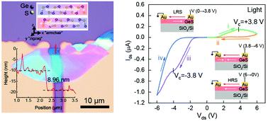
Two-dimensional ferroelectric semiconductors (2DFeSs) have been attracting extensive research attention on account of their unique properties and versatile applications in random-access memory, digital signal processors, and neuromorphic computing. Germanium sulfide (GeS) is predicted as a typical 2DFeS with a large spontaneous polarization of 484 pC m−1. Furthermore, the moderate band gap equivalent to 1.63 eV of GeS provides it with significant potential to create a strong bulk photovoltage in the visible light range. However, the fabrication of chemically stable few-to-monolayer GeS has not been reported so far, owing to the strong interlayer force and high chemical reactivity of the surface. Herein we demonstrate a new method for fabricating high quality, air-stable, ultrathin GeS nanoflakes. The electrical characterization confirms the formation of few-layered GeS with a remarkable in-plane ferroelectric hysteresis, which is forbidden by the inversion symmetry in bulk GeS crystals. After applying a coercive field of about 18.1 kV cm−1, a switchable shift current can also be observed in the polarized GeS nanoflakes under light irradiation. To further enhance the photoresponsivity, few-layered InSe was transferred onto the GeS nanoflakes to form van der Waals ferroelectric diodes. The interfacial perturbation breaking the inversion symmetry results in the enhancement of robust dipoles in the GeS side along the interface, which can be tuned by the in-plane electric field. Overall, this work opens the door for exploring the low-dimensional ferroelectric memory and energy conversion applications based on 2D GeS nanoflakes and provides a deeper understanding of the photovoltaic mechanism with in-plane 2D ferroelectric diodes.
中文翻译:

少层GeS及其范德华铁电二极管的面内铁电性
二维铁电半导体 (2DFeSs) 因其独特的性质和在随机存取存储器、数字信号处理器和神经形态计算中的广泛应用而引起了广泛的研究关注。硫化锗 (GeS) 被预测为典型的 2DFeS,具有 484 pC m -1的大自发极化. 此外,相当于 1.63 eV GeS 的中等带隙为其提供了在可见光范围内产生强体光电压的巨大潜力。然而,由于层间力强和表面的高化学反应性,迄今为止尚未报道化学稳定的少到单层 GeS 的制备。在此,我们展示了一种制造高质量、空气稳定、超薄 GeS 纳米薄片的新方法。电学表征证实了具有显着面内铁电滞后的少层 GeS 的形成,这是块状 GeS 晶体中的反转对称性所禁止的。施加约 18.1 kV cm -1的矫顽场后,在光照射下,在极化的 GeS 纳米薄片中也可以观察到可切换的位移电流。为了进一步提高光响应性,将少层 InSe 转移到 GeS 纳米薄片上以形成范德华铁电二极管。破坏反演对称性的界面扰动导致沿界面的 GeS 侧鲁棒偶极子的增强,这可以通过面内电场进行调整。总的来说,这项工作为探索基于 2D GeS 纳米薄片的低维铁电存储器和能量转换应用打开了大门,并提供了对面内 2D 铁电二极管光伏机制的更深入理解。
更新日期:2021-09-17
中文翻译:
少层GeS及其范德华铁电二极管的面内铁电性
二维铁电半导体 (2DFeSs) 因其独特的性质和在随机存取存储器、数字信号处理器和神经形态计算中的广泛应用而引起了广泛的研究关注。硫化锗 (GeS) 被预测为典型的 2DFeS,具有 484 pC m -1的大自发极化. 此外,相当于 1.63 eV GeS 的中等带隙为其提供了在可见光范围内产生强体光电压的巨大潜力。然而,由于层间力强和表面的高化学反应性,迄今为止尚未报道化学稳定的少到单层 GeS 的制备。在此,我们展示了一种制造高质量、空气稳定、超薄 GeS 纳米薄片的新方法。电学表征证实了具有显着面内铁电滞后的少层 GeS 的形成,这是块状 GeS 晶体中的反转对称性所禁止的。施加约 18.1 kV cm -1的矫顽场后,在光照射下,在极化的 GeS 纳米薄片中也可以观察到可切换的位移电流。为了进一步提高光响应性,将少层 InSe 转移到 GeS 纳米薄片上以形成范德华铁电二极管。破坏反演对称性的界面扰动导致沿界面的 GeS 侧鲁棒偶极子的增强,这可以通过面内电场进行调整。总的来说,这项工作为探索基于 2D GeS 纳米薄片的低维铁电存储器和能量转换应用打开了大门,并提供了对面内 2D 铁电二极管光伏机制的更深入理解。


 京公网安备 11010802027423号