当前位置:
X-MOL 学术
›
J. Phys. Chem. C
›
论文详情
Our official English website, www.x-mol.net, welcomes your
feedback! (Note: you will need to create a separate account there.)
Etching-Free Transfer and Nanoimaging of CVD-Grown MoS2 Monolayers
The Journal of Physical Chemistry C ( IF 3.3 ) Pub Date : 2021-09-16 , DOI: 10.1021/acs.jpcc.1c05510 Syed Hamza Safeer 1 , Thiago L. Vasconcelos 2 , Bruno S. Oliveira 2 , Braulio Soares Archanjo 2 , Michael Nazarkovsky 3 , Cecília Vilani 3 , Fernando Lazaro Freire 1 , Victor Carozo 1
The Journal of Physical Chemistry C ( IF 3.3 ) Pub Date : 2021-09-16 , DOI: 10.1021/acs.jpcc.1c05510 Syed Hamza Safeer 1 , Thiago L. Vasconcelos 2 , Bruno S. Oliveira 2 , Braulio Soares Archanjo 2 , Michael Nazarkovsky 3 , Cecília Vilani 3 , Fernando Lazaro Freire 1 , Victor Carozo 1
Affiliation
|
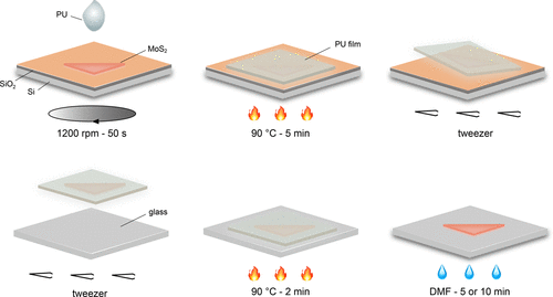
The transfer of two-dimensional materials from grown substrates onto target substrates is critical for device applications and postgrown analysis. The traditional transfer method for as-grown two-dimensional materials requires a wet chemical etching process that damages the crystals and the substrates. These issues deteriorate the electrical and optical performances of two-dimensional-material-based devices fabricated afterward. Herein, we developed an etching-free method and nanoimaging for transferring and analyzing monolayers of MoS2 onto arbitrary substrates using polyurethane as a sacrifice polymer. The polymer layer and the MoS2 crystals can be peeled off from the substrate by tweezers and transferred to any substrate. We analyzed the transferred samples to a glass coverslip substrate with optical microscopy, atomic force microscopy, tip-enhanced Raman spectroscopy, and tip-enhanced photoluminesce spectroscopy. Also, we transferred monolayers of MoS2 to a transmission electron microscopy grid and acquired scanning electron microscopy together with high-resolution scanning transmission electron microscopy images. The results of nanoimaging indicate that the method preserved the sample’s optical and structural properties and avoid undesirable cracks, wrinkles, and polymer residues. The etching-free transfer method of as-grown two-dimensional materials will improve the quality of transferred samples enhance the devices’ performance.
中文翻译:

CVD 生长的二硫化钼单层的无蚀刻转移和纳米成像
二维材料从生长基板到目标基板的转移对于器件应用和后生长分析至关重要。传统的二维材料转移方法需要湿化学蚀刻工艺,这会损坏晶体和基板。这些问题会降低随后制造的基于二维材料的器件的电学和光学性能。在此,我们开发了一种无蚀刻方法和纳米成像,用于使用聚氨酯作为牺牲聚合物将 MoS 2 的单层转移和分析到任意基材上。聚合物层和 MoS 2晶体可以用镊子从基板上剥离并转移到任何基板上。我们用光学显微镜、原子力显微镜、尖端增强拉曼光谱和尖端增强光致发光光谱分析了转移到玻璃盖玻片基底上的样品。此外,我们将单层 MoS 2转移到透射电子显微镜网格,并获得扫描电子显微镜和高分辨率扫描透射电子显微镜图像。纳米成像结果表明,该方法保留了样品的光学和结构特性,避免了不希望有的裂纹、皱纹和聚合物残留。二维材料的无蚀刻转移方法将提高转移样品的质量,增强器件的性能。
更新日期:2021-09-30
中文翻译:
CVD 生长的二硫化钼单层的无蚀刻转移和纳米成像
二维材料从生长基板到目标基板的转移对于器件应用和后生长分析至关重要。传统的二维材料转移方法需要湿化学蚀刻工艺,这会损坏晶体和基板。这些问题会降低随后制造的基于二维材料的器件的电学和光学性能。在此,我们开发了一种无蚀刻方法和纳米成像,用于使用聚氨酯作为牺牲聚合物将 MoS 2 的单层转移和分析到任意基材上。聚合物层和 MoS 2晶体可以用镊子从基板上剥离并转移到任何基板上。我们用光学显微镜、原子力显微镜、尖端增强拉曼光谱和尖端增强光致发光光谱分析了转移到玻璃盖玻片基底上的样品。此外,我们将单层 MoS 2转移到透射电子显微镜网格,并获得扫描电子显微镜和高分辨率扫描透射电子显微镜图像。纳米成像结果表明,该方法保留了样品的光学和结构特性,避免了不希望有的裂纹、皱纹和聚合物残留。二维材料的无蚀刻转移方法将提高转移样品的质量,增强器件的性能。


 京公网安备 11010802027423号