当前位置:
X-MOL 学术
›
ACS Appl. Mater. Interfaces
›
论文详情
Our official English website, www.x-mol.net, welcomes your
feedback! (Note: you will need to create a separate account there.)
Charge Storage of Isolated Monolayer Molybdenum Disulfide in Epitaxially Grown MoS2/Graphene Heterostructures for Memory Device Applications
ACS Applied Materials & Interfaces ( IF 8.3 ) Pub Date : 2021-09-14 , DOI: 10.1021/acsami.1c12064 Po-Cheng Tsai, Chun-Wei Huang, Shoou-Jinn Chang, Shu-Wei Chang, Shih-Yen Lin
ACS Applied Materials & Interfaces ( IF 8.3 ) Pub Date : 2021-09-14 , DOI: 10.1021/acsami.1c12064 Po-Cheng Tsai, Chun-Wei Huang, Shoou-Jinn Chang, Shu-Wei Chang, Shih-Yen Lin
|
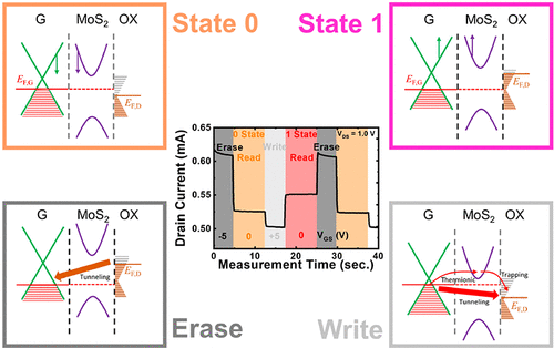
We epitaxially grew bilayer molybdenum disulfide (MoS2) on monolayer graphene by sulfurizing a molybdenum-trioxide film (MoO3) which was deposited with thermal evaporation. The Hall mobilities of graphene before and after the growth of MoS2 are similar, indicating that the underlying 2D layer was little affected during the deposition and sulfurization. Through the atomic-layer etching, the topmost layer of MoS2 is isolated from the source and drain electrodes. The top-gate transistor with the isolated monolayer MoS2 on top of the graphene channel exhibits hysteresis of drain current as the gate voltage varies. This may be due to the weak tunneling through 2D layers bonded by the van der Waals force in the absence of an external electric field. The long retention time of the device features robust charge storage around the isolated MoS2 layer. The one-transistor-zero-capacitor memory module based on this thin heterostructure of 2D materials can be advantageous for applications in dynamic random access memories with reduced thickness.
中文翻译:

用于存储器件应用的外延生长的 MoS2/石墨烯异质结构中孤立单层二硫化钼的电荷存储
我们通过硫化用热蒸发沉积的三氧化钼膜 (MoO 3 )在单层石墨烯上外延生长双层二硫化钼 (MoS 2 ) 。MoS 2生长前后石墨烯的霍尔迁移率相似,表明下面的二维层在沉积和硫化过程中几乎没有受到影响。通过原子层蚀刻,MoS 2的最顶层与源电极和漏电极隔离。具有隔离单层 MoS 2的顶栅晶体管随着栅极电压的变化,石墨烯通道顶部的 漏电流表现出滞后现象。这可能是由于在没有外部电场的情况下通过范德华力结合的二维层的弱隧道效应。该器件的长保留时间在隔离的 MoS 2层周围具有强大的电荷存储。基于这种二维材料的薄异质结构的单晶体管零电容存储器模块有利于在厚度减小的动态随机存取存储器中的应用。
更新日期:2021-09-29
中文翻译:
用于存储器件应用的外延生长的 MoS2/石墨烯异质结构中孤立单层二硫化钼的电荷存储
我们通过硫化用热蒸发沉积的三氧化钼膜 (MoO 3 )在单层石墨烯上外延生长双层二硫化钼 (MoS 2 ) 。MoS 2生长前后石墨烯的霍尔迁移率相似,表明下面的二维层在沉积和硫化过程中几乎没有受到影响。通过原子层蚀刻,MoS 2的最顶层与源电极和漏电极隔离。具有隔离单层 MoS 2的顶栅晶体管随着栅极电压的变化,石墨烯通道顶部的 漏电流表现出滞后现象。这可能是由于在没有外部电场的情况下通过范德华力结合的二维层的弱隧道效应。该器件的长保留时间在隔离的 MoS 2层周围具有强大的电荷存储。基于这种二维材料的薄异质结构的单晶体管零电容存储器模块有利于在厚度减小的动态随机存取存储器中的应用。


 京公网安备 11010802027423号