Microelectronics Journal ( IF 1.9 ) Pub Date : 2021-09-13 , DOI: 10.1016/j.mejo.2021.105246 Hossein Yaghobi 1 , Javad Tavakoli 1 , Samad Sheikhaei 1
|
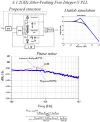
In conventional charge-pump PLLs, if the third high-frequency pole is ignored, the system comprises of two poles and a zero. The transfer function of such a system is second-order low pass, which in some part of its frequency spectrum, the amplitude response goes above unity. This translates to jitter-peaking, which in turn amplifies the input phase noise. Depending on damping factor or , this jitter-peaking could be large or small. In this paper, a dual-path PLL with an additional Voltage Controlled Delay Line (VCDL) is presented that removes the jitter-peaking by adjusting the frequency values of the zero and poles in the PLL transfer function. In this new architecture, by increasing the VCO's gain () the output phase noise is reduced. Designed and simulated in 65 nm CMOS and operating with a reference frequency of 12.5 MHz, the proposed PLL provides a spur level of −45dBc. The presented PLL exhibits an in-band phase noise of at 1 MHz offset and total power consumption of 10.5 mW.
中文翻译:
1.2 GHz 无抖动峰值的整数 N PLL
在传统的电荷泵 PLL 中,如果忽略第三个高频极点,则系统由两个极点和一个零组成。这种系统的传递函数是二阶低通函数,在其频谱的某些部分,幅度响应超越统一。这会转化为抖动峰值,进而放大输入相位噪声。取决于阻尼系数或,这种抖动峰值可能很大也可能很小。在本文中,提出了一种带有附加压控延迟线 (VCDL) 的双路径 PLL,它通过调整 PLL 传递函数中零和极点的频率值来消除抖动峰值。在这种新架构中,通过增加 VCO 的增益 () 输出相位噪声降低。在 65 nm CMOS 中设计和模拟并在 12.5 MHz 的参考频率下运行,建议的 PLL 提供 -45dBc 的杂散电平。所提出的 PLL 表现出带内相位噪声 在 1 MHz 偏移和 10.5 mW 的总功耗下。


 京公网安备 11010802027423号