Our official English website, www.x-mol.net, welcomes your
feedback! (Note: you will need to create a separate account there.)
How Thin Practical Silicon Heterojunction Solar Cells Could Be? Experimental Study under 1 Sun and under Indoor Illumination
Solar RRL ( IF 6.0 ) Pub Date : 2021-09-03 , DOI: 10.1002/solr.202100594 Ugochi Chime 1, 2 , Leon Wolf 1 , Viktoriia Buga 1 , Daniel Weigand 1 , Alaaeldin Gad 1 , Julian Köhler 1 , Andreas Lambertz 1 , Weiyuan Duan 1 , Kaining Ding 1 , Tsvetelina Merdzhanova 1 , Uwe Rau 1, 2 , Oleksandr Astakhov 1
Solar RRL ( IF 6.0 ) Pub Date : 2021-09-03 , DOI: 10.1002/solr.202100594 Ugochi Chime 1, 2 , Leon Wolf 1 , Viktoriia Buga 1 , Daniel Weigand 1 , Alaaeldin Gad 1 , Julian Köhler 1 , Andreas Lambertz 1 , Weiyuan Duan 1 , Kaining Ding 1 , Tsvetelina Merdzhanova 1 , Uwe Rau 1, 2 , Oleksandr Astakhov 1
Affiliation
|
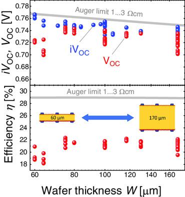
The transition toward thinner microcrystalline silicon wafers for their potential performance gain has been of interest in recent years. Theoretical predictions have estimated a maximum efficiency for silicon wafers to be at about 100−110 μm thickness. The potential and losses in silicon heterojunction solar cells prepared on wafers with thickness in the range of 60−170 μm with focus on open-circuit voltage (V
OC) and fill factor (FF) are studied experimentally. The applicability of thinner wafers for low light and indoor applications using light emitting diode (LED) lighting is also studied. The implied V
OC (iV
OC) is observed to increase with a decrease in wafer thickness according to theoretical predictions with absolute values approaching the theoretical limit. Unlike the iV
OC, the implied FF is observed to decrease with wafer thickness reduction opposite to the theoretical predictions which are related to the effect of surface recombination. A combination of gains and losses results in a broad range of high efficiency under 1 sun for wafer thicknesses ranging from 75 to 170 μm with maximum of 22.3% obtained at 75 μm. As for indoor performance, thinner wafers show slightly better efficiency at lower light intensity under sun and LED illumination, promising improved performance for even thinner devices.
中文翻译:

实用的硅异质结太阳能电池有多薄?1太阳和室内照明下的实验研究
近年来,向更薄的微晶硅晶片过渡以获得潜在的性能增益引起了人们的兴趣。理论预测估计硅晶片的最大效率约为 100-110 μm 厚度。实验研究了在厚度为 60-170 μm 的晶片上制备的硅异质结太阳能电池的电势和损耗,重点关注开路电压 ( V OC ) 和填充因子 (FF)。还研究了使用发光二极管 (LED) 照明的较薄晶圆在低光照和室内应用中的适用性。隐含的V OC ( iV OC) 根据理论预测观察到随着晶片厚度的减小而增加,绝对值接近理论极限。与iV OC不同,观察到隐含的 FF 随着晶片厚度的减小而减小,这与与表面复合效应相关的理论预测相反。增益和损耗的组合导致在 1 sun 下对于 75 至 170 μm 的晶圆厚度范围内的广泛高效率,在 75 μm 处获得的最大效率为 22.3%。至于室内性能,在阳光和 LED 照明下,较薄的晶圆在较低光强度下的效率略高,有望提高更薄设备的性能。
更新日期:2021-09-03
中文翻译:
实用的硅异质结太阳能电池有多薄?1太阳和室内照明下的实验研究
近年来,向更薄的微晶硅晶片过渡以获得潜在的性能增益引起了人们的兴趣。理论预测估计硅晶片的最大效率约为 100-110 μm 厚度。实验研究了在厚度为 60-170 μm 的晶片上制备的硅异质结太阳能电池的电势和损耗,重点关注开路电压 ( V OC ) 和填充因子 (FF)。还研究了使用发光二极管 (LED) 照明的较薄晶圆在低光照和室内应用中的适用性。隐含的V OC ( iV OC) 根据理论预测观察到随着晶片厚度的减小而增加,绝对值接近理论极限。与iV OC不同,观察到隐含的 FF 随着晶片厚度的减小而减小,这与与表面复合效应相关的理论预测相反。增益和损耗的组合导致在 1 sun 下对于 75 至 170 μm 的晶圆厚度范围内的广泛高效率,在 75 μm 处获得的最大效率为 22.3%。至于室内性能,在阳光和 LED 照明下,较薄的晶圆在较低光强度下的效率略高,有望提高更薄设备的性能。


 京公网安备 11010802027423号