Nano Research ( IF 9.5 ) Pub Date : 2021-09-02 , DOI: 10.1007/s12274-021-3785-1 Hong Li 1 , Jiakun Liang 1 , Qida Wang 1 , Fengbin Liu 1 , Gang Zhou 2 , Tao Qing 2 , Shaohua Zhang 2 , Jing Lu 3, 4, 5
|
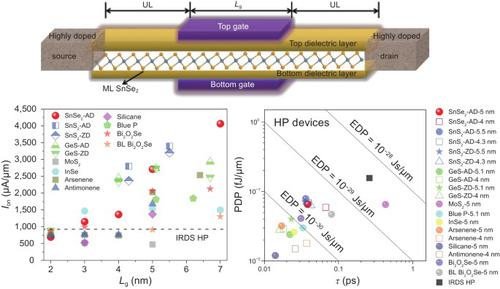
Two-dimensional (2D) semiconductors are attractive channels to shrink the scale of field-effect transistors (FETs), and among which the anisotropic one is more advantageous for a higher on-state current (Ion). Monolayer (ML) SnSe2, as an abundant, economic, nontoxic, and stable two-dimensional material, possesses an anisotropic electronic nature. Herein, we study the device performances of the ML SnSe2 metal-oxide-semiconductor FETs (MOSFETs) and deduce their performance limit to an ultrashort gate length (Lg) and ultralow supply voltage (Vdd) by using the ab initio quantum transport simulation. An ultrahigh Ion of 5,660 and 3,145 µA/µm is acquired for the n-type 10-nm-Lg ML SnSe2 MOSFET at Vdd = 0.7 V for high-performance (HP) and low-power (LP) applications, respectively. Specifically, until Lg scales down to 2 and 3 nm, the MOSFETs (at Vdd = 0.65 V) surpass Ion, intrinsic delay time (τ), and power-delay product (PDP) of the International Roadmap for Device and Systems (IRDS, 2020 version) for HP and LP devices for the year 2028. Moreover, the 5-nm-Lg ML SnSe2 MOSFET (at Vdd = 0.4 V) fulfills the IRDS HP device and the 7-nm-Lg MOSFET (at Vdd = 0.55 V) fulfills the IRDS LP device for the year 2034.
中文翻译:
单层 SnSe2 MOSFET 的器件性能极限
二维 (2D) 半导体是缩小场效应晶体管 (FET) 规模的有吸引力的通道,其中各向异性半导体更有利于更高的导通电流 ( I on )。单层 (ML) SnSe 2作为一种丰富、经济、无毒且稳定的二维材料,具有各向异性的电子性质。在此,我们研究了 ML SnSe 2金属氧化物半导体 FET (MOSFET)的器件性能,并通过使用ab initio量子传输推断其性能限制为超短栅极长度 ( L g ) 和超低电源电压 ( V dd )模拟。超高压我上对于高性能 (HP) 和低功率 (LP) 应用,在V dd = 0.7 V 时,n 型 10- nm - L g ML SnSe 2 MOSFET 分别获得了 5,660 和 3,145 µA/µm 的电流。具体来说,在L g缩小到 2 和 3 nm 之前,MOSFET(在V dd = 0.65 V 时)超过了I on、固有延迟时间 ( τ ) 和国际设备和系统路线图的功率延迟积 (PDP) (IRDS,2020 版)用于 2028 年的 HP 和 LP 器件。此外,5- nm - L g ML SnSe 2 MOSFET(在V dd= 0.4 V) 满足 IRDS HP 器件,7-nm- L g MOSFET(V dd = 0.55 V)满足 2034 年的 IRDS LP 器件。


 京公网安备 11010802027423号