Carbon ( IF 10.5 ) Pub Date : 2021-09-01 , DOI: 10.1016/j.carbon.2021.08.078 A.M. Mumlyakov 1 , M.V. Shibalov 1 , E.R. Timofeeva 1 , I.V. Trofimov 1 , N.V. Porokhov 1 , S.A. Evlashin 1 , P.A. Nekludova 1 , E.A. Pershina 1 , Yu.V. Anufriev 1 , A.M. Tagachenkov 1 , E.V. Zenova 1 , M.A. Tarkhov 1
|
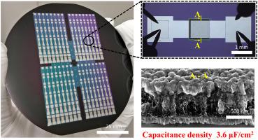
Vertically oriented graphene structures have a high specific surface area which makes them potential candidates for realization of various devices. On their basis, supercapacitors, lithium-ion batteries, absorbing coatings and bolometers, gas and electrochemical sensors, and other devices have been demonstrated. At the same time, such structures for conventional capacitors remain unexplored. In this research the fabrication technology of quasi three-dimensional capacitors based on metal/carbon nanowalls/insulator/metal structure (MCNWIM) are demonstrated. Carbon NanoWalls (CNWs) were used as a base electrode to increase the specific surface area of capacitors. Uniform dielectric and metal layers of aluminum oxide (AlOx) and titanium nitride (TiNx) were deposited by thermal atomic layer deposition (ALD) and plasma-enhanced atomic layer deposition (PEALD). A comparative analysis of capacitors with and without a carbon nanostructure has been performed. The influence of dielectric thickness on the capacitance density as well as dependencies of breakdown voltage on the surface area were experimentally observed. The maximum capacitance density was 3.6 μF/cm2 at the AlOx thickness of 10 nm, which is 4.7 times higher than the values of capacitors without carbon nanostructure. The investigated structures were manufactured on four-inch silicon wafers that provide the possibility of the mass production of capacitors based on CNWs.
中文翻译:
基于碳纳米壁的准三维电容器结构的制备与表征
垂直取向的石墨烯结构具有高比表面积,这使其成为实现各种器件的潜在候选者。在它们的基础上,超级电容器、锂离子电池、吸收涂层和辐射热计、气体和电化学传感器以及其他设备已被证明。与此同时,传统电容器的这种结构仍未得到探索。本研究展示了基于金属/碳纳米壁/绝缘体/金属结构(MCNWIM)的准三维电容器的制造技术。碳纳米壁 (CNW) 用作基础电极以增加电容器的比表面积。氧化铝 (AlO x ) 和氮化钛 (TiN x ) 的均匀介电层和金属层) 通过热原子层沉积 (ALD) 和等离子体增强原子层沉积 (PEALD) 进行沉积。对具有和不具有碳纳米结构的电容器进行了比较分析。通过实验观察了电介质厚度对电容密度的影响以及击穿电压对表面积的依赖性。在AlO x厚度为10 nm时,最大电容密度为3.6 μF/cm 2,比没有碳纳米结构的电容器的值高4.7倍。所研究的结构是在四英寸硅晶片上制造的,这为大规模生产基于 CNW 的电容器提供了可能性。


 京公网安备 11010802027423号