当前位置:
X-MOL 学术
›
ACS Appl. Electron. Mater.
›
论文详情
Our official English website, www.x-mol.net, welcomes your
feedback! (Note: you will need to create a separate account there.)
Device Characterization of Nanoscale Vertical-Channel Transistors Implemented with a Mesa-Shaped SiO2 Spacer and an In–Ga–Zn–O Active Channel
ACS Applied Electronic Materials ( IF 4.3 ) Pub Date : 2021-08-31 , DOI: 10.1021/acsaelm.1c00631 Hyun-Joo Ryoo 1 , Hyun-Min Ahn 1 , Nak-Jin Seong 2 , Kyu-Jeong Choi 2 , Chi-Sun Hwang 3 , Sung-Jin Chang 4 , Sung-Min Yoon 1
ACS Applied Electronic Materials ( IF 4.3 ) Pub Date : 2021-08-31 , DOI: 10.1021/acsaelm.1c00631 Hyun-Joo Ryoo 1 , Hyun-Min Ahn 1 , Nak-Jin Seong 2 , Kyu-Jeong Choi 2 , Chi-Sun Hwang 3 , Sung-Jin Chang 4 , Sung-Min Yoon 1
Affiliation
|
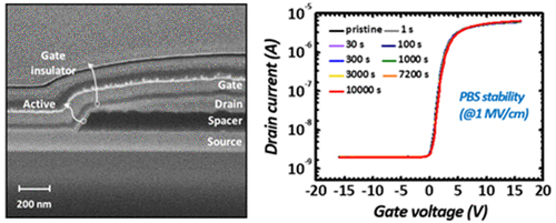
A nanoscale vertical-channel thin film transistor (V-TFT) with a channel length shorter than 160 nm was fabricated and characterized, in which In–Ga–Zn–O (IGZO) and SiO2 thin films were prepared by atomic layer deposition and plasma-enhanced chemical-vapor deposition as active and spacer layers, respectively. The prototype device showed sound transistor operation with an on/off ratio of 8.8 × 10³ and robust stabilities without any shift in transfer curves under positive/negative bias stresses at 1 MV/cm for 104 s. It was also noteworthy that there was no anomalous increase in off-state current during the positive bias stress test, which is suggested to originate from a high-quality interface between the SiO2 spacer and IGZO active layers on the back-channel region. Alternatively, high off-state current levels were found to result from the formation of conduction paths generated by carbon-related residues on the vertical back-channel region through the surface time-of-flight secondary ion mass spectrometer analysis. Improvements in device performance and analysis of operation failures will provide insight into the implementation of nanoscale oxide V-TFTs.
中文翻译:

使用台面形 SiO2 间隔物和 In-Ga-Zn-O 有源通道实现的纳米级垂直通道晶体管的器件表征
制备并表征了沟道长度小于 160 nm 的纳米级垂直沟道薄膜晶体管 (V-TFT),其中 In-Ga-Zn-O (IGZO) 和 SiO 2薄膜通过原子层沉积和等离子体增强化学气相沉积分别作为活性层和间隔层。原型设备显示出良好的晶体管操作,具有 8.8 × 10 3的开/关比和强大的稳定性,在 1 MV/cm 的正/负偏置应力下传输曲线没有任何偏移,持续 10 4秒。还值得注意的是,在正偏置应力测试期间,断态电流没有异常增加,这表明这源于 SiO 2之间的高质量界面背沟道区上的间隔层和 IGZO 有源层。或者,通过表面飞行时间二次离子质谱仪分析,发现高断态电流水平是由垂直反向通道区域上的碳相关残留物产生的传导路径形成的结果。器件性能的改进和操作故障的分析将有助于深入了解纳米级氧化物 V-TFT 的实施。
更新日期:2021-09-28
中文翻译:
使用台面形 SiO2 间隔物和 In-Ga-Zn-O 有源通道实现的纳米级垂直通道晶体管的器件表征
制备并表征了沟道长度小于 160 nm 的纳米级垂直沟道薄膜晶体管 (V-TFT),其中 In-Ga-Zn-O (IGZO) 和 SiO 2薄膜通过原子层沉积和等离子体增强化学气相沉积分别作为活性层和间隔层。原型设备显示出良好的晶体管操作,具有 8.8 × 10 3的开/关比和强大的稳定性,在 1 MV/cm 的正/负偏置应力下传输曲线没有任何偏移,持续 10 4秒。还值得注意的是,在正偏置应力测试期间,断态电流没有异常增加,这表明这源于 SiO 2之间的高质量界面背沟道区上的间隔层和 IGZO 有源层。或者,通过表面飞行时间二次离子质谱仪分析,发现高断态电流水平是由垂直反向通道区域上的碳相关残留物产生的传导路径形成的结果。器件性能的改进和操作故障的分析将有助于深入了解纳米级氧化物 V-TFT 的实施。


 京公网安备 11010802027423号