当前位置:
X-MOL 学术
›
Phys. Rev. Materials
›
论文详情
Our official English website, www.x-mol.net, welcomes your feedback! (Note: you will need to create a separate account there.)
Effect of a subnanometer thin insulator layer at the Ag/Si(111) interface through the observation of quantum well states
Physical Review Materials ( IF 3.4 ) Pub Date : 2021-08-30 , DOI: 10.1103/physrevmaterials.5.084604 R. Flammini 1 , S. Colonna 1 , P. M. Sheverdyaeva 2 , M. Papagno 3 , A. K. Kundu 4 , P. Moras 2
Physical Review Materials ( IF 3.4 ) Pub Date : 2021-08-30 , DOI: 10.1103/physrevmaterials.5.084604 R. Flammini 1 , S. Colonna 1 , P. M. Sheverdyaeva 2 , M. Papagno 3 , A. K. Kundu 4 , P. Moras 2
Affiliation
|
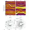
The “two-step” growth technique has been used to grow atomically uniform Ag films on Si(111) and (0001)/Si(111) surfaces. Angle-resolved photoemission spectroscopy reveals the formation of quantum well states in the Ag films with distinct properties in the two cases. It is shown that the valence electrons in silver can be confined in the fundamental gap of a less than 1-nm-thin nitride layer, effectively decoupling the Ag and Si states.
中文翻译:

通过观察量子阱态,亚纳米薄绝缘体层对 Ag/Si(111) 界面的影响
“两步”生长技术已被用于在表面上生长原子均匀的 Ag 薄膜 硅(111)和 (0001)/Si(111) 表面。角分辨光电子能谱揭示了在两种情况下具有不同性质的 Ag 薄膜中的量子阱态。结果表明,银中的价电子可以被限制在小于 1 nm 薄氮化物层的基本间隙中,有效地解耦 Ag 和 Si 状态。
更新日期:2021-08-30
中文翻译:
通过观察量子阱态,亚纳米薄绝缘体层对 Ag/Si(111) 界面的影响
“两步”生长技术已被用于在表面上生长原子均匀的 Ag 薄膜 硅(111)和 (0001)/Si(111) 表面。角分辨光电子能谱揭示了在两种情况下具有不同性质的 Ag 薄膜中的量子阱态。结果表明,银中的价电子可以被限制在小于 1 nm 薄氮化物层的基本间隙中,有效地解耦 Ag 和 Si 状态。


 京公网安备 11010802027423号