当前位置:
X-MOL 学术
›
Adv. Electron. Mater.
›
论文详情
Our official English website, www.x-mol.net, welcomes your
feedback! (Note: you will need to create a separate account there.)
In Situ Dielectric Al2O3/β-Ga2O3 Interfaces Grown Using Metal–Organic Chemical Vapor Deposition
Advanced Electronic Materials ( IF 5.3 ) Pub Date : 2021-08-28 , DOI: 10.1002/aelm.202100333 Saurav Roy 1 , Adrian E. Chmielewski 2 , Arkka Bhattacharyya 1 , Praneeth Ranga 1 , Rujun Sun 1 , Michael A. Scarpulla 1 , Nasim Alem 2 , Sriram Krishnamoorthy 1, 3
Advanced Electronic Materials ( IF 5.3 ) Pub Date : 2021-08-28 , DOI: 10.1002/aelm.202100333 Saurav Roy 1 , Adrian E. Chmielewski 2 , Arkka Bhattacharyya 1 , Praneeth Ranga 1 , Rujun Sun 1 , Michael A. Scarpulla 1 , Nasim Alem 2 , Sriram Krishnamoorthy 1, 3
Affiliation
|
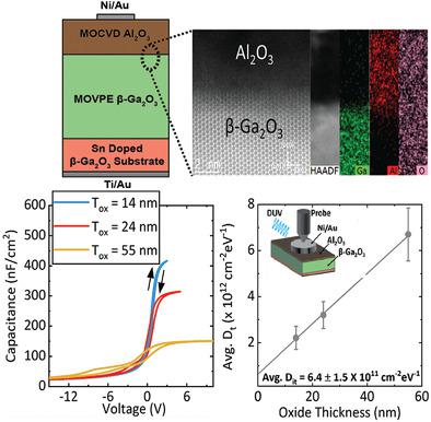
High quality dielectric-semiconductor interfaces are critical for reliable high-performance transistors. This paper reports the in situ metal–organic chemical vapor deposition of Al2O3 on β-Ga2O3 as a potentially better alternative to the most commonly used atomic layer deposition (ALD). The growth of Al2O3 is performed in the same reactor as Ga2O3 using trimethylaluminum and O2 as precursors without breaking the vacuum at a growth temperature of 600 °C. The fast and slow near interface traps at the Al2O3/β-Ga2O3 interface are identified and quantified using stressed capacitance–voltage (CV) measurements on metal oxide semiconductor capacitor (MOSCAP) structures. The density of shallow and deep level initially filled traps (Dit) are measured using ultraviolet-assisted CV technique. The average Dit for the MOSCAP is determined to be 6.4 × 1011 cm−2eV−1. The conduction band offset of the Al2O3/ Ga2O3 interface is also determined from CV measurements and found out to be 1.7 eV which is in close agreement with the existing literature reports of ALD Al2O3/Ga2O3 interface. The current–voltage characteristics are also analyzed and the average breakdown field is extracted to be approximately 5.8 MV cm−1. This in situ Al2O3 dielectric on β-Ga2O3 with improved dielectric properties can enable Ga2O3-based high-performance devices.
中文翻译:

使用金属-有机化学气相沉积法生长的原位介电 Al2O3/β-Ga2O3 界面
高质量的电介质-半导体界面对于可靠的高性能晶体管至关重要。本文报道Al的原位有机金属化学气相沉积2 ö 3上的β-Ga 2 ö 3作为潜在的更好的替代方案中最常用的原子层沉积(ALD)。Al 2 O 3的生长在与 Ga 2 O 3相同的反应器中进行,使用三甲基铝和 O 2作为前体,在 600°C 的生长温度下不破坏真空。Al 2 O 3 /β-Ga 2 O 3处的快慢近界面陷阱使用金属氧化物半导体电容器 (MOSCAP) 结构上的应力电容 - 电压 (CV) 测量来识别和量化界面。使用紫外线辅助 CV 技术测量初始填充陷阱的浅层和深层密度 (D it )。MOSCAP的平均D it被确定为6.4 × 10 11 cm -2 eV -1。Al 2 O 3 / Ga 2 O 3界面的导带偏移也由 CV 测量确定,发现为 1.7 eV,这与 ALD Al 2 O 3的现有文献报道非常一致/Ga 2 O 3界面。还分析了电流-电压特性,提取的平均击穿场约为 5.8 MV cm -1。这种在β-Ga 2 O 3 上具有改进介电性能的原位Al 2 O 3电介质可以实现基于Ga 2 O 3的高性能器件。
更新日期:2021-08-28
中文翻译:
使用金属-有机化学气相沉积法生长的原位介电 Al2O3/β-Ga2O3 界面
高质量的电介质-半导体界面对于可靠的高性能晶体管至关重要。本文报道Al的原位有机金属化学气相沉积2 ö 3上的β-Ga 2 ö 3作为潜在的更好的替代方案中最常用的原子层沉积(ALD)。Al 2 O 3的生长在与 Ga 2 O 3相同的反应器中进行,使用三甲基铝和 O 2作为前体,在 600°C 的生长温度下不破坏真空。Al 2 O 3 /β-Ga 2 O 3处的快慢近界面陷阱使用金属氧化物半导体电容器 (MOSCAP) 结构上的应力电容 - 电压 (CV) 测量来识别和量化界面。使用紫外线辅助 CV 技术测量初始填充陷阱的浅层和深层密度 (D it )。MOSCAP的平均D it被确定为6.4 × 10 11 cm -2 eV -1。Al 2 O 3 / Ga 2 O 3界面的导带偏移也由 CV 测量确定,发现为 1.7 eV,这与 ALD Al 2 O 3的现有文献报道非常一致/Ga 2 O 3界面。还分析了电流-电压特性,提取的平均击穿场约为 5.8 MV cm -1。这种在β-Ga 2 O 3 上具有改进介电性能的原位Al 2 O 3电介质可以实现基于Ga 2 O 3的高性能器件。


 京公网安备 11010802027423号