当前位置:
X-MOL 学术
›
Phys. Status Solidi B
›
论文详情
Our official English website, www.x-mol.net, welcomes your
feedback! (Note: you will need to create a separate account there.)
Damage-Free Depth Profiling of Electronic Structures in Multilayered Organic Semiconductors by Photoelectron Spectroscopy and Cluster Ion Beam
Physica Status Solidi (B) - Basic Solid State Physics ( IF 1.5 ) Pub Date : 2021-08-19 , DOI: 10.1002/pssb.202100130 Juntao Hu 1, 2 , Dengke Wang 1 , Peicheng Li 3 , Nan Chen 1 , Tao Zhang 1 , Yan Wu 1 , Di Wu 1 , Yongbiao Zhao 1 , Qiang Zhu 1 , Zewei Fu 2 , Zheng-Hong Lu 1, 3
Physica Status Solidi (B) - Basic Solid State Physics ( IF 1.5 ) Pub Date : 2021-08-19 , DOI: 10.1002/pssb.202100130 Juntao Hu 1, 2 , Dengke Wang 1 , Peicheng Li 3 , Nan Chen 1 , Tao Zhang 1 , Yan Wu 1 , Di Wu 1 , Yongbiao Zhao 1 , Qiang Zhu 1 , Zewei Fu 2 , Zheng-Hong Lu 1, 3
Affiliation
|
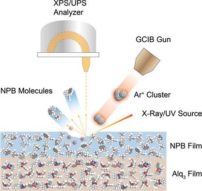
The chemical and electronic properties of multilayers are known to dictate the performance of organic semiconductor devices. Gas cluster ion beam (GCIB) is developed for removing layer-by-layer molecular materials from surfaces. It is, however, not clear whether GCIB sputter can leave a damage-free surface so that the true chemical and electronic properties can be measured. Herein, X-ray and ultraviolet photoelectron spectroscopy (XPS and UPS) are used to probe the chemical and electronic structures of organic semiconductors bombarded by GCIB. It is found that the highest occupied molecular orbitals (HOMOs) measured by UPS are very sensitive to ion-beam bombardment, whereas the XPS-measured core levels show little change. It is, therefore, essential to use UPS for determining whether the chemical and electronic properties are damaged. Of all combinations of cluster size and beam energy, it is found that 4 keV 2000 argon ion cluster can produce a fresh damage-free organic surface. Applying this optimal beam to sputter stacked films comprising tris(8-hydroxy-quinoline) aluminum (Alq3)/N,N′-bis-(1-naphthyl)-N,N′-diphenyl-1,1′-biphenyl-4,4′-diamine (NPB)/Alq3, it is shown that the chemical and electronic structures of the buried interfaces can be measured. This work demonstrates that photoelectron spectroscopies combined with GCIB can be used to construct chemical and electronic structures of multilayers in organic devices.
中文翻译:

通过光电子能谱和簇离子束对多层有机半导体中的电子结构进行无损伤深度分析
众所周知,多层膜的化学和电子特性决定了有机半导体器件的性能。气体团簇离子束 (GCIB) 被开发用于从表面逐层去除分子材料。然而,尚不清楚 GCIB 溅射是否可以留下无损伤的表面,以便可以测量真实的化学和电子特性。在此,X 射线和紫外光电子能谱(XPS 和 UPS)用于探测被 GCIB 轰击的有机半导体的化学和电子结构。结果表明,UPS 测量的最高占据分子轨道 (HOMO) 对离子束轰击非常敏感,而 XPS 测量的核心能级几乎没有变化。因此,必须使用UPS来确定化学和电子特性是否损坏。在簇大小和束能量的所有组合中,发现 4 keV 2000 氩离子簇可以产生新鲜的无损伤有机表面。将此最佳光束应用于包含三(8-羟基-喹啉)铝(Alq3 )/ N,N' -bis-(1-naphthyl)- N,N' -diphenyl-1,1 ' -biphenyl-4,4 ' -diamine (NPB)/Alq 3,表明化学式和可以测量埋入界面的电子结构。这项工作表明,光电子能谱结合 GCIB 可用于构建有机器件中多层的化学和电子结构。
更新日期:2021-08-19
中文翻译:
通过光电子能谱和簇离子束对多层有机半导体中的电子结构进行无损伤深度分析
众所周知,多层膜的化学和电子特性决定了有机半导体器件的性能。气体团簇离子束 (GCIB) 被开发用于从表面逐层去除分子材料。然而,尚不清楚 GCIB 溅射是否可以留下无损伤的表面,以便可以测量真实的化学和电子特性。在此,X 射线和紫外光电子能谱(XPS 和 UPS)用于探测被 GCIB 轰击的有机半导体的化学和电子结构。结果表明,UPS 测量的最高占据分子轨道 (HOMO) 对离子束轰击非常敏感,而 XPS 测量的核心能级几乎没有变化。因此,必须使用UPS来确定化学和电子特性是否损坏。在簇大小和束能量的所有组合中,发现 4 keV 2000 氩离子簇可以产生新鲜的无损伤有机表面。将此最佳光束应用于包含三(8-羟基-喹啉)铝(Alq3 )/ N,N' -bis-(1-naphthyl)- N,N' -diphenyl-1,1 ' -biphenyl-4,4 ' -diamine (NPB)/Alq 3,表明化学式和可以测量埋入界面的电子结构。这项工作表明,光电子能谱结合 GCIB 可用于构建有机器件中多层的化学和电子结构。


 京公网安备 11010802027423号