当前位置:
X-MOL 学术
›
Acc. Mater. Res.
›
论文详情
Our official English website, www.x-mol.net, welcomes your
feedback! (Note: you will need to create a separate account there.)
2D Bi2O2Se: An Emerging Material Platform for the Next-Generation Electronic Industry
Accounts of Materials Research ( IF 14.0 ) Pub Date : 2021-08-19 , DOI: 10.1021/accountsmr.1c00130 Tianran Li 1 , Hailin Peng 2
Accounts of Materials Research ( IF 14.0 ) Pub Date : 2021-08-19 , DOI: 10.1021/accountsmr.1c00130 Tianran Li 1 , Hailin Peng 2
Affiliation
|
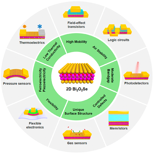
Silicon has been the dominant semiconductor for the microelectronics industry since the late 1950s. Following Moore’s law, silicon-based integrated circuit (IC) technology evolved into a 5 nm node by the end of 2020. However, silicon-based electronics face various challenges such as reduced carrier mobility and increased short-channel effects at sub-10 nm nodes. To overcome these drawbacks, two-dimensional (2D) semiconductors are among the most competitive candidate materials for next-generation electronics, due to their intrinsic atomic thickness, flexibility, and dangling-bond-free surfaces. Among all the 2D semiconductors, an air-stable and high-mobility 2D Bi2O2Se semiconductor, a novel ternary material, has some prominent advantages that make it particularly favorable in the electronics industry. First, it demonstrates ultrahigh carrier mobility, moderate band gap, outstanding stability, and excellent mechanical properties. Second, it can react with oxygen plasma or oxygen at elevated temperatures to form a high-κ native oxide Bi2SeO5. The native oxide Bi2SeO5 forms an atomically sharp interface with Bi2O2Se and can directly serve as a gate dielectric. Bi2O2Se is also embodied with some interesting physical properties such as strong spin–orbit coupling, dimerized selenium vacancies, and ferroelectricity. Taking advantage of these properties, researchers have fabricated high-performance electronic devices, including logic devices, optoelectronics, thermoelectrics, sensors, and memory devices.
中文翻译:

2D Bi2O2Se:下一代电子行业的新兴材料平台
自 1950 年代后期以来,硅一直是微电子行业的主要半导体。遵循摩尔定律,硅基集成电路 (IC) 技术到 2020 年底发展到 5 nm 节点。 然而,硅基电子产品面临各种挑战,例如载流子迁移率降低和亚 10 nm 的短沟道效应增加节点。为了克服这些缺点,二维 (2D) 半导体因其固有的原子厚度、柔韧性和无悬空键表面而成为下一代电子产品最具竞争力的候选材料之一。在所有 2D 半导体中,空气稳定和高迁移率的 2D Bi 2 O 2硒半导体是一种新型的三元材料,具有一些突出的优势,使其在电子行业中尤其受欢迎。首先,它表现出超高的载流子迁移率、适中的带隙、出色的稳定性和优异的机械性能。其次,它可以在高温下与氧等离子体或氧反应,形成高 κ 天然氧化物 Bi 2 SeO 5。原生氧化物 Bi 2 SeO 5与 Bi 2 O 2 Se形成原子级尖锐的界面,可直接用作栅极电介质。铋2 O 2Se 还具有一些有趣的物理特性,例如强自旋轨道耦合、二聚硒空位和铁电性。利用这些特性,研究人员制造了高性能电子器件,包括逻辑器件、光电子器件、热电器件、传感器和存储器件。
更新日期:2021-09-24
中文翻译:
2D Bi2O2Se:下一代电子行业的新兴材料平台
自 1950 年代后期以来,硅一直是微电子行业的主要半导体。遵循摩尔定律,硅基集成电路 (IC) 技术到 2020 年底发展到 5 nm 节点。 然而,硅基电子产品面临各种挑战,例如载流子迁移率降低和亚 10 nm 的短沟道效应增加节点。为了克服这些缺点,二维 (2D) 半导体因其固有的原子厚度、柔韧性和无悬空键表面而成为下一代电子产品最具竞争力的候选材料之一。在所有 2D 半导体中,空气稳定和高迁移率的 2D Bi 2 O 2硒半导体是一种新型的三元材料,具有一些突出的优势,使其在电子行业中尤其受欢迎。首先,它表现出超高的载流子迁移率、适中的带隙、出色的稳定性和优异的机械性能。其次,它可以在高温下与氧等离子体或氧反应,形成高 κ 天然氧化物 Bi 2 SeO 5。原生氧化物 Bi 2 SeO 5与 Bi 2 O 2 Se形成原子级尖锐的界面,可直接用作栅极电介质。铋2 O 2Se 还具有一些有趣的物理特性,例如强自旋轨道耦合、二聚硒空位和铁电性。利用这些特性,研究人员制造了高性能电子器件,包括逻辑器件、光电子器件、热电器件、传感器和存储器件。


 京公网安备 11010802027423号