Materials & Design ( IF 7.6 ) Pub Date : 2021-08-18 , DOI: 10.1016/j.matdes.2021.110052 A. Borzì 1 , R. Zboray 1 , S. Dolabella 1, 2 , J.F. Le Neal 3 , P. Drljaca 3 , G. Fiorucci 4 , A. Dommann 1 , A. Neels 1, 4
|
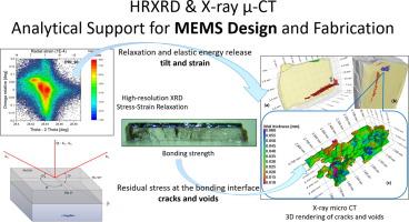
Devices such as sensors, actuators, or micro-electromechanical systems (MEMS) are obtained by a variety of microfabrication processes. Many of these processes influence the material systems by the introduction of strain and defects, which may affect the final device's performance and reliability. Indeed, controlling materials' status during the microfabrication is fundamental for the process optimization itself and for guaranteeing the highest devices performances during their lifetime. In this work, a conjoint analytical approach between high-resolution X-ray diffraction (HRXRD) and X-ray micro-computed tomography (CT) evaluates an innovative silicon-to-sapphire wafer bonding process. Large cracks 30–60 µm-thick were identified in both crystals by micro-CT and related to the interfacial high-stress release. In parallel, a multi-domain microstructure associated with strain and tilt affect the silicon crystallinity due to smaller cracks and defects which originate at the bonding interface and travel to the outer part of the crystal. The effectiveness of the bonding is also assessed by our approach and further enforced by means of SEM observation of the sample cross-section. Here, a unique approach by combining X-ray micro CT with HRXRD for a holistic evaluation of silicon-to-sapphire wafer-bonding processes and correlate the micrometer scale and volumetric defect detection (voids and cracks) with atomic-level strain and defect analysis is presented.
中文翻译:
支持传感器设计和制造的整体 X 射线分析方法:晶圆键合工艺的应变和裂纹分析
传感器、执行器或微机电系统 (MEMS) 等设备是通过各种微制造工艺获得的。许多这些过程通过引入应变和缺陷来影响材料系统,这可能会影响最终设备的性能和可靠性。事实上,在微制造过程中控制材料的状态是工艺优化本身和保证设备在其生命周期内达到最高性能的基础。在这项工作中,高分辨率 X 射线衍射 (HRXRD) 和 X 射线显微计算机断层扫描 (CT) 之间的联合分析方法评估了一种创新的硅-蓝宝石晶片键合工艺。通过显微 CT 在两种晶体中都发现了 30-60 µm 厚的大裂纹,并且与界面高应力释放有关。在平行下,与应变和倾斜相关的多域微观结构会影响硅的结晶度,因为较小的裂纹和缺陷起源于键合界面并传播到晶体的外部。粘合的有效性也通过我们的方法进行评估,并通过对样品横截面的 SEM 观察进一步加强。在这里,一种独特的方法将 X 射线显微 CT 与 HRXRD 相结合,对硅-蓝宝石晶片键合工艺进行整体评估,并将微米尺度和体积缺陷检测(空隙和裂纹)与原子级应变和缺陷分析相关联被表达。粘合的有效性也通过我们的方法进行评估,并通过对样品横截面的 SEM 观察进一步加强。在这里,一种独特的方法将 X 射线显微 CT 与 HRXRD 相结合,对硅-蓝宝石晶片键合工艺进行整体评估,并将微米尺度和体积缺陷检测(空隙和裂纹)与原子级应变和缺陷分析相关联被表达。粘合的有效性也通过我们的方法进行评估,并通过对样品横截面的 SEM 观察进一步加强。在这里,一种独特的方法将 X 射线显微 CT 与 HRXRD 相结合,对硅-蓝宝石晶片键合工艺进行整体评估,并将微米尺度和体积缺陷检测(空隙和裂纹)与原子级应变和缺陷分析相关联被表达。


 京公网安备 11010802027423号