Microelectronic Engineering ( IF 2.6 ) Pub Date : 2021-08-17 , DOI: 10.1016/j.mee.2021.111616 M. Hochedel 1 , M. Bichotte 1, 2 , F. Arnould 1 , F. Celle 1 , C. Veillas 1 , T. Pouit 2 , L. Dubost 2 , T. Kämpfe 1 , O. Dellea 3 , N. Crespo-Monteiro 1 , Y. Jourlin 1
|
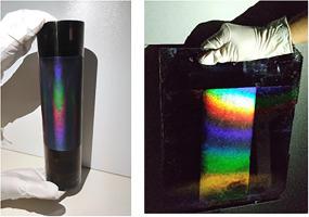
This paper presents an innovative fabrication process of microstructured spectrally selective solar absorbers for concentrated solar power (CSP) plants. The authors describe suitable technologies and methods to microstructure large areas and non-conventional substrates, such as tubes, and substrates with large surface areas typically used in CSP plants. Specific colloidal lithography combined with layer deposition makes it possible to structure this type of substrate with a submicron periodicity within a hexagonal arrangement. Appropriate techniques, e.g. Langmuir-Blodgett deposition and customized UV insolation were developed to process 80 mm diameter and 300 mm long tubes and 300 × 300 mm2 planar substrates. Absorbing and anti-reflection coatings were deposited using industrial vacuum deposition equipment with three different deposition sources: PECVD, magnetron sputtering and cathodic arc deposition. The design and assessment of the efficiency of the microstructure absorbing layers on smaller planar substrates are described elsewhere, assuming that optical performances are close to the large and tubular substrates. The technological processes and the resulting demonstrators are described in detail herein.
中文翻译:
用于聚光太阳能发电厂 (CSP) 的大型圆柱形接收器的微结构技术
本文介绍了一种用于聚光太阳能 (CSP) 发电厂的微结构光谱选择性太阳能吸收器的创新制造工艺。作者描述了对大面积和非常规基材进行微结构化的合适技术和方法,例如管子,以及通常用于 CSP 工厂的大表面积基材。特定的胶体光刻与层沉积相结合,可以在六边形排列内构造具有亚微米周期性的这种类型的基板。开发了适当的技术,例如 Langmuir-Blodgett 沉积和定制的紫外线照射,以处理直径为 80 毫米、长为 300 毫米的管子和 300 × 300 毫米2平面基板。使用具有三种不同沉积源的工业真空沉积设备沉积吸收和抗反射涂层:PECVD、磁控溅射和阴极电弧沉积。假设光学性能接近大型和管状基板,在其他地方描述了对较小平面基板上的微结构吸收层的效率的设计和评估。本文详细描述了技术过程和由此产生的演示器。


 京公网安备 11010802027423号