当前位置:
X-MOL 学术
›
Phys. Status Solidi B
›
论文详情
Our official English website, www.x-mol.net, welcomes your
feedback! (Note: you will need to create a separate account there.)
Empty Valence-Band Pocket in p-Type Cu2O(111) Probed with Scanning Tunneling Spectroscopy
Physica Status Solidi (B) - Basic Solid State Physics ( IF 1.5 ) Pub Date : 2021-08-10 , DOI: 10.1002/pssb.202100337 Alexander Gloystein 1 , Niklas Nilius 1
Physica Status Solidi (B) - Basic Solid State Physics ( IF 1.5 ) Pub Date : 2021-08-10 , DOI: 10.1002/pssb.202100337 Alexander Gloystein 1 , Niklas Nilius 1
Affiliation
|
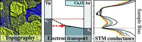
Scanning tunneling spectroscopy is used to probe the surface electronic structure of (√3×√3)-reconstructed cuprous oxide films on Au(111). In analogy to bulk Cu2O(111), the films show a pronounced p-type nature with the valence-band top pinned to the Fermi level and the conduction-band onset located at +2.0 V. A conductance dip appears directly at zero bias in the dI/dV spectra, followed by an asymmetric dI/dV maximum inside the lower half of the bandgap. Several scenarios are considered to explain this unusual conductance behavior. The most likely interpretation is based on the accumulation of hole states in the p-type material in response to the tip-electric field and the development of an empty valence-band pocket directly below the tip. Tunneling into these states leads to a finite dI/dV intensity even inside the Cu2O bandgap. A 1D tunneling model that accounts for this field-dependent transport mechanism successfully reproduces the experimental data and rationalizes the impact of current setpoint, oxide thickness, and surface reconstruction on the observed spectral response.
中文翻译:

用扫描隧道光谱法探测 p 型 Cu2O(111) 中的空价带袋
扫描隧道光谱用于探测Au(111)上(√3×√3)-重构氧化亚铜薄膜的表面电子结构。与块体 Cu 2 O(111)类似,薄膜显示出明显的 p 型性质,价带顶部固定在费米能级上,导带起始点位于 +2.0 V。电导下降直接出现在零处d I /d V光谱中的偏差,然后是不对称的 d I /d V在带隙的下半部分内达到最大值。几种情况被认为可以解释这种不寻常的电导行为。最可能的解释是基于 p 型材料中空穴态的积累,以响应尖端电场和尖端正下方空价带袋的发展。即使在 Cu 2 O 带隙内部,隧道进入这些状态也会导致有限的 d I /d V强度。解释这种场相关传输机制的一维隧道模型成功地再现了实验数据,并使电流设定点、氧化物厚度和表面重建对观察到的光谱响应的影响合理化。
更新日期:2021-08-10
中文翻译:
用扫描隧道光谱法探测 p 型 Cu2O(111) 中的空价带袋
扫描隧道光谱用于探测Au(111)上(√3×√3)-重构氧化亚铜薄膜的表面电子结构。与块体 Cu 2 O(111)类似,薄膜显示出明显的 p 型性质,价带顶部固定在费米能级上,导带起始点位于 +2.0 V。电导下降直接出现在零处d I /d V光谱中的偏差,然后是不对称的 d I /d V在带隙的下半部分内达到最大值。几种情况被认为可以解释这种不寻常的电导行为。最可能的解释是基于 p 型材料中空穴态的积累,以响应尖端电场和尖端正下方空价带袋的发展。即使在 Cu 2 O 带隙内部,隧道进入这些状态也会导致有限的 d I /d V强度。解释这种场相关传输机制的一维隧道模型成功地再现了实验数据,并使电流设定点、氧化物厚度和表面重建对观察到的光谱响应的影响合理化。


 京公网安备 11010802027423号