当前位置:
X-MOL 学术
›
Inorg. Chem. Front.
›
论文详情
Our official English website, www.x-mol.net, welcomes your
feedback! (Note: you will need to create a separate account there.)
Surface-dependent band structure variations and bond-level deviations in Cu2O
Inorganic Chemistry Frontiers ( IF 6.1 ) Pub Date : 2021-07-22 , DOI: 10.1039/d1qi00733e Chih-Shan Tan, Michael H. Huang
Inorganic Chemistry Frontiers ( IF 6.1 ) Pub Date : 2021-07-22 , DOI: 10.1039/d1qi00733e Chih-Shan Tan, Michael H. Huang
|
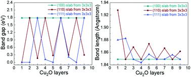
Density functional theory (DFT) calculations have been performed on 1 to 9 layers of Cu2O (100), (111), and (110) planes to further understand the electronic band structures and the origin of the facet-dependent properties of Cu2O crystals. The (100) planes show an invariant band structure with a constant band gap of 1.787 eV like that of a primitive cell. The (111) planes present a periodicity of every three layers with band gaps varying between zero and 1.787 eV. An unusual periodicity of every two layers has been found for the (110) planes oscillating between 1.787 eV and very small band gaps including a zero band gap. By comparing the valence band edges of different plane layers and the position of the Fermi level in the density of states (DOS) diagrams, relative valence band bending of the Cu2O {100}, {111}, and {110} surfaces can be drawn to explain their strongly facet-dependent electrical conductivity properties. Moreover, while the (100) planes show a fixed crystal lattice with a tunable number of planes, the calculations identify slight bond length deviations and bond distortion for the (111) and (110) planes. The partial density of states (PDOS) diagrams also reveal (111) and (110) plane layer-dependent variations in the frontier orbital electron energy distribution. The structural perturbations at crystal surfaces can yield different barrier heights to charge transport across the {100}, {111}, and {110} faces, and photons of different wavelengths should get absorbed in the thin surface layer to produce the observed optical facet effects. Such lattice perturbations should be present in other semiconductor materials as surface-dependent behaviors are broadly observable in many semiconductors.
中文翻译:

Cu2O 中与表面相关的能带结构变化和键能级偏差
已对 1 到 9 层 Cu 2 O (100)、(111) 和 (110) 平面进行密度泛函理论 (DFT) 计算,以进一步了解 Cu 的电子能带结构和面相关特性的起源2哦水晶。(100) 平面显示出恒定带隙为 1.787 eV 的不变带结构,就像原始电池的带隙一样。(111) 平面呈现出每三层的周期性,带隙在 0 到 1.787 eV 之间变化。对于在 1.787 eV 和非常小的带隙(包括零带隙)之间振荡的 (110) 平面,发现了每两层的不寻常周期性。通过比较不同平面层的价带边缘和费米能级在态密度(DOS)图中的位置,Cu 2 的相对价带弯曲可以绘制 O {100}、{111} 和 {110} 表面来解释它们强烈依赖于小平面的导电特性。此外,虽然 (100) 平面显示固定晶格和可调平面数,但计算确定了 (111) 和 (110) 平面的轻微键长偏差和键变形。部分态密度 (PDOS) 图还揭示了前沿轨道电子能量分布的 (111) 和 (110) 平面层相关变化。晶体表面的结构扰动可以产生不同的势垒高度以跨越 {100}、{111} 和 {110} 面进行电荷传输,并且不同波长的光子应该在薄表面层中被吸收以产生观察到的光学面效应.
更新日期:2021-08-09
中文翻译:
Cu2O 中与表面相关的能带结构变化和键能级偏差
已对 1 到 9 层 Cu 2 O (100)、(111) 和 (110) 平面进行密度泛函理论 (DFT) 计算,以进一步了解 Cu 的电子能带结构和面相关特性的起源2哦水晶。(100) 平面显示出恒定带隙为 1.787 eV 的不变带结构,就像原始电池的带隙一样。(111) 平面呈现出每三层的周期性,带隙在 0 到 1.787 eV 之间变化。对于在 1.787 eV 和非常小的带隙(包括零带隙)之间振荡的 (110) 平面,发现了每两层的不寻常周期性。通过比较不同平面层的价带边缘和费米能级在态密度(DOS)图中的位置,Cu 2 的相对价带弯曲可以绘制 O {100}、{111} 和 {110} 表面来解释它们强烈依赖于小平面的导电特性。此外,虽然 (100) 平面显示固定晶格和可调平面数,但计算确定了 (111) 和 (110) 平面的轻微键长偏差和键变形。部分态密度 (PDOS) 图还揭示了前沿轨道电子能量分布的 (111) 和 (110) 平面层相关变化。晶体表面的结构扰动可以产生不同的势垒高度以跨越 {100}、{111} 和 {110} 面进行电荷传输,并且不同波长的光子应该在薄表面层中被吸收以产生观察到的光学面效应.


 京公网安备 11010802027423号