Our official English website, www.x-mol.net, welcomes your
feedback! (Note: you will need to create a separate account there.)
Toward Unusual-High Hole Mobility of p-Channel Field-Effect-Transistors
Small ( IF 13.0 ) Pub Date : 2021-07-19 , DOI: 10.1002/smll.202102323 Jiamin Sun 1, 2 , Xinming Zhuang 1 , Yibo Fan 1 , Shuai Guo 3 , Zichao Cheng 4 , Dong Liu 1, 2 , Yanxue Yin 1 , Yufeng Tian 1 , Zhiyong Pang 1 , Zhipeng Wei 3 , Xiufeng Song 4 , Lei Liao 5 , Feng Chen 1 , Johnny C Ho 6 , Zai-Xing Yang 1, 2
Small ( IF 13.0 ) Pub Date : 2021-07-19 , DOI: 10.1002/smll.202102323 Jiamin Sun 1, 2 , Xinming Zhuang 1 , Yibo Fan 1 , Shuai Guo 3 , Zichao Cheng 4 , Dong Liu 1, 2 , Yanxue Yin 1 , Yufeng Tian 1 , Zhiyong Pang 1 , Zhipeng Wei 3 , Xiufeng Song 4 , Lei Liao 5 , Feng Chen 1 , Johnny C Ho 6 , Zai-Xing Yang 1, 2
Affiliation
|
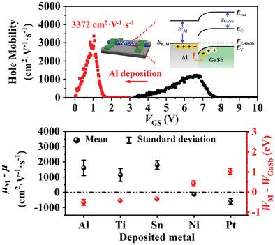
The relative low hole mobility of p-channel building block device challenges the continued miniaturization of modern electronic chips. Metal-semiconductor junction is always an efficient strategy to control the carrier concentration of channel semiconductor, benefiting the carrier mobility regulation of building block device. In this work, complementary metal oxide semiconductor (CMOS)-compatible metals are selected to deposit on the surface of the important p-channel building block of GaSb nanowire field-effect-transistors (NWFETs), demonstrating the efficient strategy of hole mobility enhancement by metal-semiconductor junction. When deposited with lower work function metal of Al, the peak hole mobility of GaSb NWFET can be enhanced to as high as ≈3372 cm2 V−1 s−1, showing three times than the un-deposited one. The as-studied metal-semiconductor junction is also efficient for the hole mobility enhancement of other p-channel devices, such as GaAs NWFET, GaAs film FET, and WSe2 FET. With the enhanced mobility, the as-constructed CMOS inverter shows good invert characteristics, showing a relatively high gain of ≈18.1. All results may be regarded as important advances to the next-generation electronics.
中文翻译:

实现 p 沟道场效应晶体管的异常高空穴迁移率
p 通道积木器件相对较低的空穴迁移率挑战了现代电子芯片的持续小型化。金属-半导体结一直是控制沟道半导体载流子浓度的有效策略,有利于积木器件的载流子迁移率调节。在这项工作中,选择与互补金属氧化物半导体 (CMOS) 兼容的金属沉积在 GaSb 纳米线场效应晶体管 (NWFET) 的重要 p 沟道构建块的表面上,证明了通过以下方式增强空穴迁移率的有效策略金属半导体结。当用 Al 的低功函数金属沉积时,GaSb NWFET 的峰值空穴迁移率可以提高到 ≈3372 cm 2 V -1 s -1,显示为未沉积的三倍。所研究的金属-半导体结对于增强其他 p 沟道器件的空穴迁移率也很有效,例如 GaAs NWFET、GaAs 薄膜 FET 和 WSe 2 FET。随着迁移率的增强,所构建的 CMOS 反相器显示出良好的反相特性,显示出 ≈18.1 的相对较高的增益。所有结果都可以被视为下一代电子产品的重要进步。
更新日期:2021-09-16
中文翻译:
实现 p 沟道场效应晶体管的异常高空穴迁移率
p 通道积木器件相对较低的空穴迁移率挑战了现代电子芯片的持续小型化。金属-半导体结一直是控制沟道半导体载流子浓度的有效策略,有利于积木器件的载流子迁移率调节。在这项工作中,选择与互补金属氧化物半导体 (CMOS) 兼容的金属沉积在 GaSb 纳米线场效应晶体管 (NWFET) 的重要 p 沟道构建块的表面上,证明了通过以下方式增强空穴迁移率的有效策略金属半导体结。当用 Al 的低功函数金属沉积时,GaSb NWFET 的峰值空穴迁移率可以提高到 ≈3372 cm 2 V -1 s -1,显示为未沉积的三倍。所研究的金属-半导体结对于增强其他 p 沟道器件的空穴迁移率也很有效,例如 GaAs NWFET、GaAs 薄膜 FET 和 WSe 2 FET。随着迁移率的增强,所构建的 CMOS 反相器显示出良好的反相特性,显示出 ≈18.1 的相对较高的增益。所有结果都可以被视为下一代电子产品的重要进步。


 京公网安备 11010802027423号