当前位置:
X-MOL 学术
›
ACS Mater. Lett.
›
论文详情
Our official English website, www.x-mol.net, welcomes your
feedback! (Note: you will need to create a separate account there.)
Large-Area Periodic Organic–Inorganic Hybrid Perovskite Nanopyramid Arrays for High-Performance Photodetector and Image Sensor Applications
ACS Materials Letters ( IF 9.6 ) Pub Date : 2021-07-08 , DOI: 10.1021/acsmaterialslett.1c00298 Xiuzhen Xu 1 , Wenfei Liu 2 , Zhenkai Ji 1 , Dandan Hao 1 , Wenyuan Yan 1 , Zilong Ye 1 , Yan Hu 1 , Minghe Fang 1 , Changchun Wang 3 , Liang Ma 4 , Jia Huang 1 , Xiaobin Xu 1 , Paul S. Weiss 2, 5
ACS Materials Letters ( IF 9.6 ) Pub Date : 2021-07-08 , DOI: 10.1021/acsmaterialslett.1c00298 Xiuzhen Xu 1 , Wenfei Liu 2 , Zhenkai Ji 1 , Dandan Hao 1 , Wenyuan Yan 1 , Zilong Ye 1 , Yan Hu 1 , Minghe Fang 1 , Changchun Wang 3 , Liang Ma 4 , Jia Huang 1 , Xiaobin Xu 1 , Paul S. Weiss 2, 5
Affiliation
|
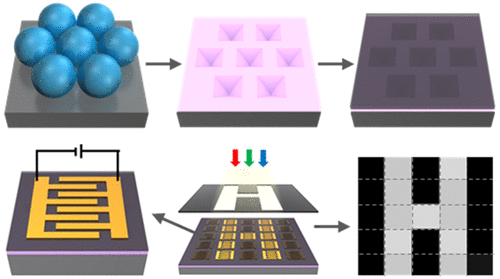
The rapid growth of organic–inorganic hybrid perovskite materials (such as methylammonium lead triiodide, MAPbI3) in photoelectric applications has prompted investigations of novel strategies to improve photodetection performance. Although a few surface nanofabrication methods have been applied to texture perovskite thin films to enhance light trapping, it remains challenging to pattern large-area periodic perovskite nanoarrays in a tunable and scalable manner. In this work, we report a facile and low-cost approach to fabricate large-area SiO2/Si nanopyramids arrays through nanosphere lithography. These nanopyramids arrays are used to pattern MAPbI3 thin films. We find that the introduction of nanopyramid arrays enhances the light intensity within the perovskite film, which is confirmed by light absorption tests and optical simulations. As a result, the photodetectors based on MAPbI3 with nanopyramid structures show excellent responsivity of 28.8 ± 1.0 A/W and detectivity of (3.5 ± 0.1) × 1011 Jones at 650 nm. The photoresponse of the photodetector to pulsed light is highly stable and reproducible, with rise and decay times of ∼0.7 and 1.1 ms, respectively. They also have a broader light sensitivity range from ultraviolet to infrared light, i.e., 340 nm to 1100 nm, compared to those without nanostructures. Finally, we demonstrate a prototype image sensor using these photodetector arrays.
中文翻译:

用于高性能光电探测器和图像传感器应用的大面积周期性有机-无机混合钙钛矿纳米金字塔阵列
有机-无机杂化钙钛矿材料(如甲基铵三碘化铅,MAPbI 3)在光电应用中的快速增长促使人们研究提高光电检测性能的新策略。尽管一些表面纳米加工方法已应用于纹理钙钛矿薄膜以增强光捕获,但以可调和可扩展的方式对大面积周期性钙钛矿纳米阵列进行图案化仍然具有挑战性。在这项工作中,我们报告了一种通过纳米球光刻制造大面积 SiO 2 /Si 纳米金字塔阵列的简便且低成本的方法。这些纳米金字塔阵列用于图案化 MAPbI 3薄膜。我们发现纳米金字塔阵列的引入增强了钙钛矿薄膜内的光强度,这通过光吸收测试和光学模拟得到证实。结果,基于具有纳米锥体结构的MAPbI 3的光电探测器显示出28.8 ± 1.0 A/W 的出色响应度和650 nm 处的(3.5 ± 0.1) × 10 11 Jones探测率。光电探测器对脉冲光的光响应高度稳定且可重复,上升和衰减时间分别为~0.7 和 1.1 ms。与没有纳米结构的那些相比,它们还具有从紫外光到红外光的更宽的光敏度范围,即 340 nm 到 1100 nm。最后,我们展示了使用这些光电探测器阵列的原型图像传感器。
更新日期:2021-08-02
中文翻译:
用于高性能光电探测器和图像传感器应用的大面积周期性有机-无机混合钙钛矿纳米金字塔阵列
有机-无机杂化钙钛矿材料(如甲基铵三碘化铅,MAPbI 3)在光电应用中的快速增长促使人们研究提高光电检测性能的新策略。尽管一些表面纳米加工方法已应用于纹理钙钛矿薄膜以增强光捕获,但以可调和可扩展的方式对大面积周期性钙钛矿纳米阵列进行图案化仍然具有挑战性。在这项工作中,我们报告了一种通过纳米球光刻制造大面积 SiO 2 /Si 纳米金字塔阵列的简便且低成本的方法。这些纳米金字塔阵列用于图案化 MAPbI 3薄膜。我们发现纳米金字塔阵列的引入增强了钙钛矿薄膜内的光强度,这通过光吸收测试和光学模拟得到证实。结果,基于具有纳米锥体结构的MAPbI 3的光电探测器显示出28.8 ± 1.0 A/W 的出色响应度和650 nm 处的(3.5 ± 0.1) × 10 11 Jones探测率。光电探测器对脉冲光的光响应高度稳定且可重复,上升和衰减时间分别为~0.7 和 1.1 ms。与没有纳米结构的那些相比,它们还具有从紫外光到红外光的更宽的光敏度范围,即 340 nm 到 1100 nm。最后,我们展示了使用这些光电探测器阵列的原型图像传感器。


 京公网安备 11010802027423号