Microelectronic Engineering ( IF 2.6 ) Pub Date : 2021-07-08 , DOI: 10.1016/j.mee.2021.111596 Mingsai Zhu 1, 2 , Yuying Xie 1, 2 , Jianan Deng 1, 2 , Yifang Chen 1 , Chongyu Mei 3
|
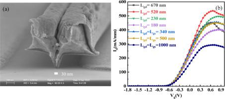
To enable mass production of InP-HEMTs operating in microwave and THz bands with T shaped gates as narrow as 30 nm, industry friendly processes for source/drain contacts are urgently needed. So far, although a self-aligned technique using pre-fabricated T shaped gates as masks has been reported, the limited adjustments of the gate-source/gate-drain spacings by this process restricts the device performance optimization. In this work, 30 nm T shaped gates by a novel bilayer of RE650/UV5 are successfully fabricated. Using the T shaped gates as masks, a self-aligned process with angled evaporation of contacts has been developed, which offers us a new degree of freedom to adjust the locations of the contacts in a large range for the optimization of the device structure. By numerical simulations, the influences of the gate-source/gate-drain spacings on the device performance such as the DC/RF characteristics, the spatial distributions of both electric fields and the carrier density, etc., have been studied. The property of InP-HEMTs with the contacts by the traditional alignment is also compared. Optimized spacings for maximizing the device performances are figured out. The progress achieved in this work should be an important guide in both the manufacturing process development and the construction of the device structure.
中文翻译:
一种调节 InP-HEMT 栅漏间距的新工艺
为了能够大规模生产在微波和太赫兹频段工作的 InP-HEMT,T 形栅极窄至 30 nm,迫切需要工业友好的源极/漏极接触工艺。到目前为止,虽然已经报道了使用预制 T 形栅极作为掩膜的自对准技术,但该工艺对栅极-源极/栅极-漏极间距的有限调整限制了器件性能优化。在这项工作中,成功制造了由新型 RE650/UV5 双层构成的 30 nm T 形栅极。使用 T 形栅极作为掩膜,开发了具有接触角蒸发的自对准工艺,这为我们提供了新的自由度,可以在大范围内调整接触位置以优化器件结构。通过数值模拟,研究了栅源/栅漏间距对器件性能的影响,如DC/RF特性、电场空间分布和载流子密度等。还比较了 InP-HEMT 与传统对准接触的特性。计算出用于最大化设备性能的优化间距。这项工作取得的进展应该对制造工艺开发和器件结构的构建具有重要的指导意义。


 京公网安备 11010802027423号