当前位置:
X-MOL 学术
›
Phys. Status Solidi A
›
论文详情
Our official English website, www.x-mol.net, welcomes your
feedback! (Note: you will need to create a separate account there.)
Defect Characterization in High-Electron-Mobility Transistors with Regrown p-GaN Gate by Low-Frequency Noise and Deep-Level Transient Spectroscopy
Physica Status Solidi (A) - Applications and Materials Science Pub Date : 2021-07-02 , DOI: 10.1002/pssa.202100227 Po-Chun (Brent) Hsu 1, 2 , Eddy Simoen 1, 3 , Hu Liang 1 , Brice De Jaeger 1 , Benoit Bakeroot 1, 4 , Dirk Wellekens 1 , Stefaan Decoutere 1
Physica Status Solidi (A) - Applications and Materials Science Pub Date : 2021-07-02 , DOI: 10.1002/pssa.202100227 Po-Chun (Brent) Hsu 1, 2 , Eddy Simoen 1, 3 , Hu Liang 1 , Brice De Jaeger 1 , Benoit Bakeroot 1, 4 , Dirk Wellekens 1 , Stefaan Decoutere 1
Affiliation
|
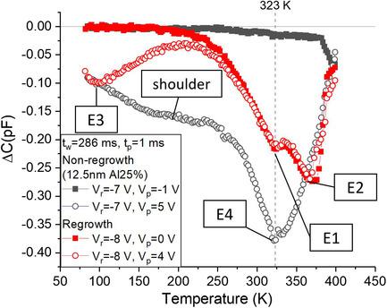
To investigate the defects from the gate regrowth process, samples with and without regrowth p-GaN process are fabricated by metalorganic chemical vapor deposition (MOCVD). The DC characteristics indicate larger gate leakage (Igs) between the GaN channel and the p-GaN gate in the regrowth sample than in the nonregrowth counterpart. In addition, significant Si/O impurities are introduced by the regrowth process at the interface between channel and regrown AlGaN barrier. The low-frequency noise (LFN) measurement and deep-level transient spectroscopy (DLTS) are further carried out to investigate the defectivity at the AlGaN barrier and channel interface, giving a 2–3 times higher border trap density in the AlGaN barrier (depth ≈5 nm from the channel interface) and a 10 times increase in interface trap density at the channel interface, corresponding with a band of shallow levels E3 = Ec–0.02–0.15 eV. Three additional bulk traps E2/E5 (Ec–0.8 eV, / Ec–0.17 eV, ) and E4 (Ec–0.23 eV, ) are also found in the regrowth and nonregrowth samples, respectively. Their possible spatial locations and origins are discussed.
中文翻译:

通过低频噪声和深能级瞬态光谱表征具有再生 p-GaN 栅极的高电子迁移率晶体管的缺陷
为了研究栅极再生长工艺中的缺陷,通过金属有机化学气相沉积 (MOCVD) 制造了采用和不采用再生长 p-GaN 工艺的样品。DC 特性表明更大的栅极泄漏 ( I gs) 在再生长样品中的 GaN 沟道和 p-GaN 栅极之间比在非再生长样品中。此外,再生长过程在沟道和再生长的 AlGaN 势垒之间的界面处引入了大量的 Si/O 杂质。进一步进行低频噪声 (LFN) 测量和深能级瞬态光谱 (DLTS) 以研究 AlGaN 势垒和沟道界面处的缺陷,使 AlGaN 势垒中的边界陷阱密度(深度≈5 nm),通道界面处的界面陷阱密度增加了 10 倍,对应于浅能级带 E3 = E c –0.02–0.15 eV。三个额外的体阱 E2/E5 ( E c –0.8 eV,/ E c –0.17 eV,) 和 E4 ( E c –0.23 eV,) 也分别出现在再生和非再生样品中。讨论了它们可能的空间位置和起源。
更新日期:2021-07-02
中文翻译:
通过低频噪声和深能级瞬态光谱表征具有再生 p-GaN 栅极的高电子迁移率晶体管的缺陷
为了研究栅极再生长工艺中的缺陷,通过金属有机化学气相沉积 (MOCVD) 制造了采用和不采用再生长 p-GaN 工艺的样品。DC 特性表明更大的栅极泄漏 ( I gs) 在再生长样品中的 GaN 沟道和 p-GaN 栅极之间比在非再生长样品中。此外,再生长过程在沟道和再生长的 AlGaN 势垒之间的界面处引入了大量的 Si/O 杂质。进一步进行低频噪声 (LFN) 测量和深能级瞬态光谱 (DLTS) 以研究 AlGaN 势垒和沟道界面处的缺陷,使 AlGaN 势垒中的边界陷阱密度(深度≈5 nm),通道界面处的界面陷阱密度增加了 10 倍,对应于浅能级带 E3 = E c –0.02–0.15 eV。三个额外的体阱 E2/E5 ( E c –0.8 eV,/ E c –0.17 eV,) 和 E4 ( E c –0.23 eV,) 也分别出现在再生和非再生样品中。讨论了它们可能的空间位置和起源。


 京公网安备 11010802027423号