Colloid and Interface Science Communications ( IF 4.5 ) Pub Date : 2021-06-26 , DOI: 10.1016/j.colcom.2021.100452 Philipp Yu. Gorobtsov , Nikita A. Fisenko , Valentin R. Solovey , Nikolay P. Simonenko , Elizaveta P. Simonenko , Ivan A. Volkov , Vladimir G. Sevastyanov , Nikolay T. Kuznetsov
|
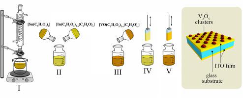
Sol-gel synthesis of thin In2O3-xSnO2 (x = 5–15 mol% SnO2) films and double-layer (In2O3-10%SnO2)/V2O5 nanostructures utilizing hydrolytically active metal alkoxoacetylacetonate complexes [M(C5H7O2)x(C4H9O)y] (M = In3+, Sn4+) and [VO(C5H7O2)2-z(C4H9O)z] as precursors was studied. Dependencies of mean coherent scattering regions (CSR) and particle size, specific resistance, work function, band gap and transmittance in visible region on tin dioxide contents in obtained In2O3-xSnO2 films were determined and attributed to changes in crystal lattice parameter and oxygen vacancies amount. For (In2O3-10%SnO2)/V2O5 bilayer thin film nanostructures, microstructural and local electrophysical properties were studied. It was shown that vanadium (V) oxide deposited on the surface of In2O3-10%SnO2 film constitutes a coating made of hemispherical clusters of about 180 nm diameter and mean height of 80 nm, with distance between clusters being roughly 100–500 nm and clusters themselves showing good conductivity.
中文翻译:
溶胶-凝胶衍生(In 2 O 3 -10%SnO 2)/V 2 O 5薄膜的微观结构和局部电物理性能
利用水解活性金属溶胶-凝胶合成薄 In 2 O 3 -xSnO 2 (x = 5–15 mol% SnO 2 ) 薄膜和双层 (In 2 O 3 -10%SnO 2 )/V 2 O 5纳米结构烷氧乙酰丙酮络合物 [M(C 5 H 7 O 2 ) x (C 4 H 9 O) y ] (M = In 3+ , Sn 4+ ) 和 [VO(C 5 H 7 O 2 ) 2-z (C 4 H9 O) z ] 作为前体进行了研究。确定了平均相干散射区 (CSR) 和粒径、电阻率、功函数、带隙和可见光区透射率对所得 In 2 O 3 -xSnO 2薄膜中二氧化锡含量的依赖性,并将其归因于晶格参数的变化和氧空位量。对于(In 2 O 3 -10%SnO 2 )/V 2 O 5双层薄膜纳米结构,研究了微观结构和局部电物理特性。结果表明,钒(V)氧化物沉积在In 2 O 3 -10%SnO表面2薄膜构成由直径约 180 nm 和平均高度为 80 nm 的半球形簇制成的涂层,簇之间的距离约为 100-500 nm,簇本身显示出良好的导电性。


 京公网安备 11010802027423号