Micro and Nanostructures ( IF 2.7 ) Pub Date : 2021-06-26 , DOI: 10.1016/j.spmi.2021.106978 Zhenguo Zhuo , Fei Yang , Junnan Han , Xincheng Cao , Yue Tao , Le Zhang , Wenjin Liu , Ziyue Zhu , Yuehua Dai
|
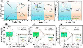
The effect of substitutional doping at S site on the electronic properties of MoS2/Graphene (MoS2/G) was studied by First-principles calculations. Through the analysis on the energy band and density of states of MoS2/Graphene, it was found that the S vacancy in MoS2 monolayer caused the Dirac point shifted, and produced the defect energy levels at the Dirac point, which hindered the carrier transmission. Periods II-IV elements were doped at the S vacancy to improve the electronic properties and performance of MoS2/G. The calculated results show that the charge transfer of MoS2/G was greatly enhanced by the doping of N, P and As atoms. The current-voltage characteristic of N, P and As-doped G/MoS2/MoS2/G structure has higher drive-current and stable OFF-state current which can reduce device current consumption. For O-doped and Se-doped MoS2/G heterostructures, there is no impurity level introduced, and the Schottky barrier height increase (decrease) with the increase (decrease) of the biaxial strain, meantime the p-type Schottky contact, n-type Schottky contact and Ohmic contact characteristic can be converted mutually by adjusting biaxial strain or vertical external force. Our findings will be of great guiding significance for the designing of interface devices and explorations on nano-electronics.
中文翻译:
MoS 2 /G异质结构S位的取代掺杂:对电压-电流和电子特性的影响
通过第一性原理计算研究了S位置换掺杂对MoS 2 /石墨烯(MoS 2 /G)电子性质的影响。通过对MoS 2 /石墨烯能带和态密度的分析,发现MoS 2单层中的S空位引起狄拉克点位移,并在狄拉克点产生缺陷能级,阻碍载流子传输. 在S空位处掺杂II-IV期元素以改善MoS 2 /G的电子性质和性能。计算结果表明,MoS 2的电荷转移N、P 和 As 原子的掺杂大大增强了 /G。N、P和As掺杂的G/MoS 2 /MoS 2 /G结构的电流-电压特性具有更高的驱动电流和稳定的关态电流,可以降低器件电流消耗。对于O掺杂和Se掺杂的MoS 2 /G异质结构,没有引入杂质能级,肖特基势垒高度随着双轴应变的增加(减少)而增加(减少),同时p型肖特基接触,n型肖特基接触和欧姆接触特性可以通过调节双轴应变或垂直外力相互转换。我们的发现对接口器件的设计和纳米电子学的探索具有重要的指导意义。


 京公网安备 11010802027423号