当前位置:
X-MOL 学术
›
Laser Photonics Rev.
›
论文详情
Our official English website, www.x-mol.net, welcomes your
feedback! (Note: you will need to create a separate account there.)
Femtosecond Field-Driven On-Chip Unidirectional Electronic Currents in Nonadiabatic Tunneling Regime
Laser & Photonics Reviews ( IF 9.8 ) Pub Date : 2021-06-16 , DOI: 10.1002/lpor.202000475 Liping Shi 1, 2 , Ihar Babushkin 3, 4, 5 , Anton Husakou 5 , Oliver Melchert 3, 4 , Bettina Frank 6 , Juemin Yi 7 , Gustav Wetzel 8 , Ayhan Demircan 3, 4 , Christoph Lienau 7 , Harald Giessen 6 , Misha Ivanov 5 , Uwe Morgner 3, 4 , Milutin Kovacev 3, 4
Laser & Photonics Reviews ( IF 9.8 ) Pub Date : 2021-06-16 , DOI: 10.1002/lpor.202000475 Liping Shi 1, 2 , Ihar Babushkin 3, 4, 5 , Anton Husakou 5 , Oliver Melchert 3, 4 , Bettina Frank 6 , Juemin Yi 7 , Gustav Wetzel 8 , Ayhan Demircan 3, 4 , Christoph Lienau 7 , Harald Giessen 6 , Misha Ivanov 5 , Uwe Morgner 3, 4 , Milutin Kovacev 3, 4
Affiliation
|
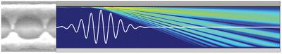
Recently, asymmetric plasmonic nanojunctions have shown promise as on-chip electronic devices to convert femtosecond optical pulses to current bursts, with a bandwidth of multi-terahertz scale, although yet at low temperatures and pressures. Such nanoscale devices are of great interest for novel ultrafast electronics and opto-electronic applications. Here, the device is operated in air and at room temperature, revealing the mechanisms of photoemission from plasmonic nanojunctions, and the fundamental limitations on the speed of optical-to-electronic conversion. Inter-cycle interference of coherent electronic wavepackets results in a complex energy electron distribution and birth of multiphoton effects. This energy structure, as well as reshaping of the wavepackets during their propagation from one tip to the other, determine the ultrafast dynamics of the current. It is shown that, up to some level of approximation, the electron flight time is well-determined by the mean ponderomotive velocity in the driving field.
中文翻译:

非绝热隧道机制中的飞秒场驱动片上单向电子电流
最近,不对称等离子体纳米结已显示出作为片上电子器件的前景,可将飞秒光脉冲转换为电流爆发,具有多太赫兹尺度的带宽,但仍处于低温和低压下。这种纳米级器件对新型超快电子和光电应用具有重要意义。在这里,该设备在空气和室温下运行,揭示了等离子体纳米结的光电发射机制,以及光电转换速度的基本限制。相干电子波包的周期间干扰导致复杂的能量电子分布和多光子效应的诞生。这种能量结构,以及波包在从一个尖端传播到另一个尖端期间的重塑,确定电流的超快动力学。结果表明,在一定程度的近似值内,电子飞行时间由驱动场中的平均有质动力速度很好地确定。
更新日期:2021-08-15
中文翻译:
非绝热隧道机制中的飞秒场驱动片上单向电子电流
最近,不对称等离子体纳米结已显示出作为片上电子器件的前景,可将飞秒光脉冲转换为电流爆发,具有多太赫兹尺度的带宽,但仍处于低温和低压下。这种纳米级器件对新型超快电子和光电应用具有重要意义。在这里,该设备在空气和室温下运行,揭示了等离子体纳米结的光电发射机制,以及光电转换速度的基本限制。相干电子波包的周期间干扰导致复杂的能量电子分布和多光子效应的诞生。这种能量结构,以及波包在从一个尖端传播到另一个尖端期间的重塑,确定电流的超快动力学。结果表明,在一定程度的近似值内,电子飞行时间由驱动场中的平均有质动力速度很好地确定。


 京公网安备 11010802027423号