当前位置:
X-MOL 学术
›
J. Appl. Crystallogr.
›
论文详情
Our official English website, www.x-mol.net, welcomes your
feedback! (Note: you will need to create a separate account there.)
X-ray rocking curve imaging on large arrays of extremely tall SiGe microcrystals epitaxial on Si
Journal of Applied Crystallography ( IF 5.2 ) Pub Date : 2021-06-14 , DOI: 10.1107/s1600576721004969 Mojmír Meduňa , Ondřej Caha , Emanuil Choumas , Franco Bressan , Hans von Känel
Journal of Applied Crystallography ( IF 5.2 ) Pub Date : 2021-06-14 , DOI: 10.1107/s1600576721004969 Mojmír Meduňa , Ondřej Caha , Emanuil Choumas , Franco Bressan , Hans von Känel
|
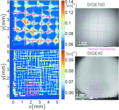
This work investigates layers of densely spaced SiGe microcrystals epitaxially formed on patterned Si and grown up to extreme heights of 40 and 100 µm using the rocking curve imaging technique with standard laboratory equipment and a 2D X-ray pixel detector. As the crystalline tilt varied both within the epitaxial SiGe layers and inside the individual microcrystals, it was possible to obtain real-space 2D maps of the local lattice bending and distortion across the complete SiGe surface. These X-ray maps, showing the variation of crystalline quality along the sample surface, were compared with optical and scanning electron microscopy images. Knowing the distribution of the X-ray diffraction peak intensity, peak position and peak width immediately yields the crystal lattice bending locally present in the samples as a result of the thermal processes arising during the growth. The results found here by a macroscopic-scale imaging technique reveal that the array of large microcrystals, which tend to fuse at a certain height, forms domains limited by cracks during cooling after the growth. The domains are characterized by uniform lattice bending and their boundaries are observed as higher distortion of the crystal structure. The effect of concave thermal lattice bending inside the microcrystal array is in excellent agreement with the results previously presented on a microscopic scale using scanning nanodiffraction.
中文翻译:

在 Si 上外延的超高 SiGe 微晶大阵列上的 X 射线摇摆曲线成像
这项工作使用摇摆曲线成像技术和标准实验室设备和 2D X 射线像素探测器,研究了在图案化的 Si 上外延形成并生长到 40 和 100 µm 的极端高度的密集间隔的 SiGe 微晶层。由于晶体倾斜在外延 SiGe 层内和单个微晶内发生变化,因此可以获得整个 SiGe 表面局部晶格弯曲和畸变的实空间二维图。这些 X 射线图显示了沿样品表面结晶质量的变化,并与光学和扫描电子显微镜图像进行了比较。知道X射线衍射峰强度的分布,由于生长过程中出现的热过程,峰位置和峰宽立即产生了样品中局部存在的晶格弯曲。通过宏观尺度成像技术发现的结果表明,倾向于在一定高度融合的大微晶体阵列在生长后的冷却过程中形成受裂纹限制的区域。域的特征在于均匀的晶格弯曲,并且观察到它们的边界是晶体结构的更高畸变。微晶阵列内凹热晶格弯曲的影响与先前使用扫描纳米衍射在微观尺度上呈现的结果非常一致。趋于在一定高度融合,在生长后的冷却过程中形成受裂纹限制的域。域的特征在于均匀的晶格弯曲,并且观察到它们的边界是晶体结构的更高畸变。微晶阵列内凹热晶格弯曲的影响与先前使用扫描纳米衍射在微观尺度上呈现的结果非常一致。趋于在一定高度融合,在生长后的冷却过程中形成受裂纹限制的域。域的特征在于均匀的晶格弯曲,并且观察到它们的边界是晶体结构的更高畸变。微晶阵列内凹热晶格弯曲的影响与先前使用扫描纳米衍射在微观尺度上呈现的结果非常一致。
更新日期:2021-08-05
中文翻译:
在 Si 上外延的超高 SiGe 微晶大阵列上的 X 射线摇摆曲线成像
这项工作使用摇摆曲线成像技术和标准实验室设备和 2D X 射线像素探测器,研究了在图案化的 Si 上外延形成并生长到 40 和 100 µm 的极端高度的密集间隔的 SiGe 微晶层。由于晶体倾斜在外延 SiGe 层内和单个微晶内发生变化,因此可以获得整个 SiGe 表面局部晶格弯曲和畸变的实空间二维图。这些 X 射线图显示了沿样品表面结晶质量的变化,并与光学和扫描电子显微镜图像进行了比较。知道X射线衍射峰强度的分布,由于生长过程中出现的热过程,峰位置和峰宽立即产生了样品中局部存在的晶格弯曲。通过宏观尺度成像技术发现的结果表明,倾向于在一定高度融合的大微晶体阵列在生长后的冷却过程中形成受裂纹限制的区域。域的特征在于均匀的晶格弯曲,并且观察到它们的边界是晶体结构的更高畸变。微晶阵列内凹热晶格弯曲的影响与先前使用扫描纳米衍射在微观尺度上呈现的结果非常一致。趋于在一定高度融合,在生长后的冷却过程中形成受裂纹限制的域。域的特征在于均匀的晶格弯曲,并且观察到它们的边界是晶体结构的更高畸变。微晶阵列内凹热晶格弯曲的影响与先前使用扫描纳米衍射在微观尺度上呈现的结果非常一致。趋于在一定高度融合,在生长后的冷却过程中形成受裂纹限制的域。域的特征在于均匀的晶格弯曲,并且观察到它们的边界是晶体结构的更高畸变。微晶阵列内凹热晶格弯曲的影响与先前使用扫描纳米衍射在微观尺度上呈现的结果非常一致。


 京公网安备 11010802027423号