Materials Today Physics ( IF 10.0 ) Pub Date : 2021-06-11 , DOI: 10.1016/j.mtphys.2021.100454 Dan Mu , Wei Zhou , Yundan Liu , Jin Li , Ming Yang , Jincheng Zhuang , Yi Du , Jianxin Zhong
|
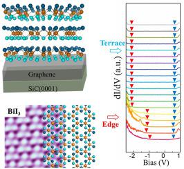
Two-dimensional materials with layered structures, appropriate bandgap, and high carrier mobilities have gathered tremendous interests due to their potential applications in optoelectronic and photovoltaic devices. Here, we report the growth of BiI3 thin film with controllable atomic thickness on graphene-terminated 6H–SiC(0001) substrate by molecular beam epitaxy (MBE) method. The growth kinetic processes and crystalline properties of the BiI3 film are studied by scanning tunneling microscopy (STM). The scanning tunneling spectroscopy (STS) reveals a bandgap of 2.8 eV for monolayer BiI3 with a weak dependence on film thickness for few-layer BiI3, which greatly exceeds the previous reported values identified by macroscopic optical measurements. This discrepancy originates from the edge effect of BiI3 that renders the bandgap downshift to 1.5–1.6 eV, as identified by the STS curves and the further confirmed by density functional theory (DFT) calculations. Our work provides a method to fabricate high-quality monolayer BiI3 film and resolves its intrinsic bandgap as well as the edge effect on reduction of bandgap, benefitting not only to fundamental researches but also to nanoelectronic and optoelectronic applications.
中文翻译:
解决在石墨烯上外延生长的 BiI 3薄膜的固有带隙和边缘效应
具有层状结构、适当带隙和高载流子迁移率的二维材料由于其在光电和光伏器件中的潜在应用而引起了极大的兴趣。在这里,我们报告了通过分子束外延 (MBE) 方法在石墨烯封端的 6H-SiC(0001) 衬底上生长原子厚度可控的 BiI 3薄膜。通过扫描隧道显微镜 (STM) 研究了 BiI 3膜的生长动力学过程和结晶特性。扫描隧道谱(STS)揭示了为2.8eV为单层BII的带隙3与膜厚的弱依赖性为少层BII 3,大大超过了先前通过宏观光学测量确定的报告值。这种差异源于 BiI 3的边缘效应,它使带隙下降到 1.5-1.6 eV,如 STS 曲线所确定的那样,密度泛函理论 (DFT) 计算进一步证实了这一点。我们的工作提供了一种制备高质量单层BiI 3薄膜的方法,并解决了其固有带隙以及减小带隙的边缘效应,不仅有利于基础研究,而且有利于纳米电子和光电应用。


 京公网安备 11010802027423号