当前位置:
X-MOL 学术
›
ACS Photonics
›
论文详情
Our official English website, www.x-mol.net, welcomes your
feedback! (Note: you will need to create a separate account there.)
Silicon-Based Quantum Mechanical Tunnel Junction for Plasmon Excitation from Low-Energy Electron Tunneling
ACS Photonics ( IF 6.5 ) Pub Date : 2021-06-09 , DOI: 10.1021/acsphotonics.0c01913 Fangwei Wang 1 , Yan Liu 2 , Thorin Jake Duffin 1, 3 , Vijith Kalathingal 1, 4 , Siping Gao 2 , Wenrui Hu 2 , Yongxin Guo 2 , Soo-Jin Chua 2, 5 , Christian A. Nijhuis 1, 3, 4, 6
ACS Photonics ( IF 6.5 ) Pub Date : 2021-06-09 , DOI: 10.1021/acsphotonics.0c01913 Fangwei Wang 1 , Yan Liu 2 , Thorin Jake Duffin 1, 3 , Vijith Kalathingal 1, 4 , Siping Gao 2 , Wenrui Hu 2 , Yongxin Guo 2 , Soo-Jin Chua 2, 5 , Christian A. Nijhuis 1, 3, 4, 6
Affiliation
|
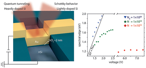
Light emission from metal–insulator–semiconductor junctions (MISJs) has been explored for decades as a possible on-chip light source; however it is not clear whether the mechanism of light emission is plasmonic in nature or is dominated by electroluminescence. Previous studies only investigated silicon with low doping levels, but here we show that only highly doped silicon allows us to excite surface plasmon polaritons (SPPs) in MISJs via inelastic tunneling. This paper describes the mechanism of charge transport and light emission from silicon-based Au-SiO2-nSi MISJs as a function of the doping level Nd varying from 1.6 × 1015 cm–3 to 1.0 × 1020 cm–3. At low doping levels (Nd ∼ 1015 cm–3), the MISJs behave as Schottky diodes, and the mechanism of light emission involves a radiative recombination of electrons and holes from minority carrier injection under high applied bias (>5.5 V). With increasing doping levels, the current–voltage characteristics of the MISJs change, resulting in symmetrical current–voltage curves with parabolic conductance behavior characteristic of quantum mechanical tunneling. MISJs with the highest doping level (Nd ∼ 1020 cm–3) are dominated by quantum mechanical tunneling, and light emission originates from radiative decay of surface plasmon polaritons (SPPs) via scattering at threshold voltages as low as 1.5 V. Our simulations indicate that tunneling over the thin SiO2 barrier between the Au and highly doped nSi excites a hybrid-SPP mode localized to the Au whose dispersion depends on the effective index induced by the SiO2–nSi interface. Our studies show that Si needs to be sufficiently doped to be conductive enough to enable SPP excitation via inelastic tunneling.
中文翻译:

用于低能电子隧道激发等离子体的硅基量子机械隧道结
金属-绝缘体-半导体结 (MISJ) 的光发射作为一种可能的片上光源已被探索了数十年。然而,目前尚不清楚光发射的机制是等离子激元还是电致发光。以前的研究只研究了低掺杂水平的硅,但在这里我们表明只有高度掺杂的硅才能通过非弹性隧道效应激发 MISJ 中的表面等离子体激元 (SPP)。本文描述了从 1.6 × 10 15 cm –3到 1.0 × 10 20 cm –3随掺杂水平N d变化的硅基 Au-SiO 2 -nSi MISJs的电荷传输和发光机制. 在低掺杂水平 ( N d ∼ 10 15 cm –3 ) 下,MISJ 表现为肖特基二极管,发光机制涉及在高施加偏压 (>5.5 V) 下少数载流子注入产生的电子和空穴的辐射复合。随着掺杂水平的增加,MISJs的电流-电压特性发生变化,导致对称的电流-电压曲线具有量子力学隧穿的抛物线电导特性。具有最高掺杂水平 ( N d ∼ 10 20 cm –3) 以量子力学隧穿为主,光发射源自表面等离子体激元 (SPP) 的辐射衰减,通过在低至 1.5 V 的阈值电压下进行散射。我们的模拟表明,在 Au 和高掺杂之间的薄 SiO 2势垒上隧穿nSi 激发了一种定位于 Au 的混合 SPP 模式,其色散取决于由 SiO 2 -nSi 界面引起的有效指数。我们的研究表明,Si 需要被充分掺杂以具有足够的导电性,才能通过非弹性隧道效应激发 SPP。
更新日期:2021-07-21
中文翻译:
用于低能电子隧道激发等离子体的硅基量子机械隧道结
金属-绝缘体-半导体结 (MISJ) 的光发射作为一种可能的片上光源已被探索了数十年。然而,目前尚不清楚光发射的机制是等离子激元还是电致发光。以前的研究只研究了低掺杂水平的硅,但在这里我们表明只有高度掺杂的硅才能通过非弹性隧道效应激发 MISJ 中的表面等离子体激元 (SPP)。本文描述了从 1.6 × 10 15 cm –3到 1.0 × 10 20 cm –3随掺杂水平N d变化的硅基 Au-SiO 2 -nSi MISJs的电荷传输和发光机制. 在低掺杂水平 ( N d ∼ 10 15 cm –3 ) 下,MISJ 表现为肖特基二极管,发光机制涉及在高施加偏压 (>5.5 V) 下少数载流子注入产生的电子和空穴的辐射复合。随着掺杂水平的增加,MISJs的电流-电压特性发生变化,导致对称的电流-电压曲线具有量子力学隧穿的抛物线电导特性。具有最高掺杂水平 ( N d ∼ 10 20 cm –3) 以量子力学隧穿为主,光发射源自表面等离子体激元 (SPP) 的辐射衰减,通过在低至 1.5 V 的阈值电压下进行散射。我们的模拟表明,在 Au 和高掺杂之间的薄 SiO 2势垒上隧穿nSi 激发了一种定位于 Au 的混合 SPP 模式,其色散取决于由 SiO 2 -nSi 界面引起的有效指数。我们的研究表明,Si 需要被充分掺杂以具有足够的导电性,才能通过非弹性隧道效应激发 SPP。


 京公网安备 11010802027423号