当前位置:
X-MOL 学术
›
Int. J. Circ. Theory Appl.
›
论文详情
Our official English website, www.x-mol.net, welcomes your
feedback! (Note: you will need to create a separate account there.)
Power and area-efficient static current mode logic frequency divider in 180-nm complementary metal-oxide-semiconductor technology
International Journal of Circuit Theory and Applications ( IF 1.8 ) Pub Date : 2021-06-08 , DOI: 10.1002/cta.3081 Subhanil Maity 1 , Sanjay Kumar Jana 1 , Indranil Som 2 , Tarun Kanti Bhattacharyya 2
International Journal of Circuit Theory and Applications ( IF 1.8 ) Pub Date : 2021-06-08 , DOI: 10.1002/cta.3081 Subhanil Maity 1 , Sanjay Kumar Jana 1 , Indranil Som 2 , Tarun Kanti Bhattacharyya 2
Affiliation
|
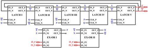
This paper presents power and area optimized, high-speed metal-oxide-semiconductor (MOS) current mode logic (MCML)-based frequency dividers. Each differential pair in the divider is sized separately to minimize the overall power consumption. The divide-by-2 frequency divider has been realized in a 180-nm complementary MOS (CMOS) process technology, and postlayout simulation results show that the proposed frequency divider can work up to an operating frequency of 18.8 GHz in the worst-case process corner with a maximum power dissipation of 1.715 mW under 1.8-V supply. It gives a bandwidth of 19.9 GHz which ranges from 1 to 20.9 GHz. The divider occupies a 0.106 × 0.09 mm2 area. The performance corresponds to the figure of merit (FoM) of 43.61 dB. The same optimized latches and two EX-OR gates are used to design a divide-by-5 frequency divider that is also realized in 180-nm CMOS process technology. The postlayout simulation results show that the proposed divide-by-5 frequency divider can faithfully work up to an operating frequency of 12.12 GHz in worst-case process corner with an excellent power head performance. The maximum power dissipation of the core circuit is 1.39 mW under 1.8-V supply. It occupies a 0.166 × 0.116 mm2 area. The performance corresponds to the FoM of 26.56 dB which compares favorably with the state of the art.
中文翻译:

采用 180 纳米互补金属氧化物半导体技术的功率和面积高效的静态电流模式逻辑分频器
本文介绍了功率和面积优化的、基于高速金属氧化物半导体 (MOS) 电流模式逻辑 (MCML) 的分频器。分频器中的每个差分对都单独调整大小,以最大限度地降低总功耗。在 180 nm 互补 MOS (CMOS) 工艺技术中实现了 2 分频分频器,布局后仿真结果表明,所提出的分频器在最坏情况下可以工作到 18.8 GHz 的工作频率在 1.8V 电源下最大功耗为 1.715 mW。它提供 19.9 GHz 的带宽,范围从 1 到 20.9 GHz。分频器占地 0.106 × 0.09 mm 2区域。性能对应于 43.61 dB 的品质因数 (FoM)。相同的优化锁存器和两个异或门用于设计一个 5 分频分频器,该分频器也采用 180 纳米 CMOS 工艺技术实现。布局后仿真结果表明,所提出的 5 分频分频器可以在最坏情况下的工艺角忠实地工作到 12.12 GHz 的工作频率,并具有出色的动力头性能。在 1.8V 电源下,核心电路的最大功耗为 1.39 mW。它占据了 0.166 × 0.116 mm 2 的面积。性能对应于 26.56 dB 的 FoM,与现有技术相比毫不逊色。
更新日期:2021-08-12
中文翻译:
采用 180 纳米互补金属氧化物半导体技术的功率和面积高效的静态电流模式逻辑分频器
本文介绍了功率和面积优化的、基于高速金属氧化物半导体 (MOS) 电流模式逻辑 (MCML) 的分频器。分频器中的每个差分对都单独调整大小,以最大限度地降低总功耗。在 180 nm 互补 MOS (CMOS) 工艺技术中实现了 2 分频分频器,布局后仿真结果表明,所提出的分频器在最坏情况下可以工作到 18.8 GHz 的工作频率在 1.8V 电源下最大功耗为 1.715 mW。它提供 19.9 GHz 的带宽,范围从 1 到 20.9 GHz。分频器占地 0.106 × 0.09 mm 2区域。性能对应于 43.61 dB 的品质因数 (FoM)。相同的优化锁存器和两个异或门用于设计一个 5 分频分频器,该分频器也采用 180 纳米 CMOS 工艺技术实现。布局后仿真结果表明,所提出的 5 分频分频器可以在最坏情况下的工艺角忠实地工作到 12.12 GHz 的工作频率,并具有出色的动力头性能。在 1.8V 电源下,核心电路的最大功耗为 1.39 mW。它占据了 0.166 × 0.116 mm 2 的面积。性能对应于 26.56 dB 的 FoM,与现有技术相比毫不逊色。


 京公网安备 11010802027423号