当前位置:
X-MOL 学术
›
Int. J. Circ. Theory Appl.
›
论文详情
Our official English website, www.x-mol.net, welcomes your
feedback! (Note: you will need to create a separate account there.)
Developed configuration of stacked multicell topology with reduced DC voltage sources
International Journal of Circuit Theory and Applications ( IF 1.8 ) Pub Date : 2021-06-07 , DOI: 10.1002/cta.3040 Sara Hazrati 1 , Mohammad Bagher Bannae Sharifian 1 , Mohammad Reza Feyzi 1 , Ebrahim Babaei 1, 2
International Journal of Circuit Theory and Applications ( IF 1.8 ) Pub Date : 2021-06-07 , DOI: 10.1002/cta.3040 Sara Hazrati 1 , Mohammad Bagher Bannae Sharifian 1 , Mohammad Reza Feyzi 1 , Ebrahim Babaei 1, 2
Affiliation
|
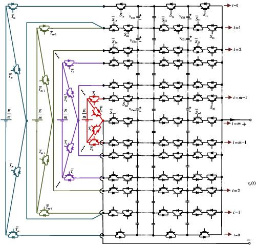
Multilevel inverters are considered as a suitable alternative for the two-level topology in the medium-voltage, high-power applications because of the higher number of voltage levels, and, as a result, reduced harmonic distortion. One of the most critical types of multilevel inverters is the flying capacitor topology, in which the stacked multicell topology is derived from this type of multilevel inverters. This paper presents a developed configuration of the stacked multicell topology, constructed from 2m × n primary commutation cells, which generates the output voltage of (2m × n)+1 levels. The most crucial point in the flying capacitor-based topologies is balancing the flying capacitors' voltages, which is the primary condition of these topologies' correct operation. Also, in this topology, the number of required DC voltage sources is decreased compared to the existing multicell topology. Moreover, the developed topology can generate a higher number of voltage levels without cascading several cells. The developed multicell inverter topology is controlled based on the disposition band carrier and phase-shifted carrier sinusoidal pulse width modulation (DBC-PSC-SPWM) method. Because of this control method, the voltages of capacitors are self-adjusted at their value. The proposed topology is simulated in different conditions using PSCAD/EMTDC software and to show the validity of the proposed topology and the control method, and simulation results are demonstrated. A laboratory-type experimental setup is used to validate the modulation strategy and other findings.
中文翻译:

具有降低的直流电压源的堆叠多单元拓扑的开发配置
多电平逆变器被认为是中压、大功率应用中两电平拓扑的合适替代方案,因为电压电平数量较多,因此谐波失真减少。最关键的多电平逆变器类型之一是飞电容拓扑,其中堆叠多单元拓扑源自这种类型的多电平逆变器。本文介绍了堆叠多单元拓扑的开发配置,由 2 m × n初级换向单元构成,产生 (2 m × n)+1 级。基于飞跨电容器的拓扑中最关键的一点是平衡飞电容器的电压,这是这些拓扑正确运行的主要条件。此外,在这种拓扑中,与现有的多单元拓扑相比,所需的直流电压源的数量减少了。此外,开发的拓扑结构可以产生更多的电压电平,而无需级联多个单元。开发的多单元逆变器拓扑基于配置带载波和相移载波正弦脉宽调制 (DBC-PSC-SPWM) 方法进行控制。由于这种控制方法,电容器的电压会自动调整到它们的值。使用 PSCAD/EMTDC 软件在不同条件下对所提出的拓扑结构进行了仿真,以证明所提出的拓扑结构和控制方法的有效性,并展示了仿真结果。实验室类型的实验装置用于验证调制策略和其他发现。
更新日期:2021-06-07
中文翻译:
具有降低的直流电压源的堆叠多单元拓扑的开发配置
多电平逆变器被认为是中压、大功率应用中两电平拓扑的合适替代方案,因为电压电平数量较多,因此谐波失真减少。最关键的多电平逆变器类型之一是飞电容拓扑,其中堆叠多单元拓扑源自这种类型的多电平逆变器。本文介绍了堆叠多单元拓扑的开发配置,由 2 m × n初级换向单元构成,产生 (2 m × n)+1 级。基于飞跨电容器的拓扑中最关键的一点是平衡飞电容器的电压,这是这些拓扑正确运行的主要条件。此外,在这种拓扑中,与现有的多单元拓扑相比,所需的直流电压源的数量减少了。此外,开发的拓扑结构可以产生更多的电压电平,而无需级联多个单元。开发的多单元逆变器拓扑基于配置带载波和相移载波正弦脉宽调制 (DBC-PSC-SPWM) 方法进行控制。由于这种控制方法,电容器的电压会自动调整到它们的值。使用 PSCAD/EMTDC 软件在不同条件下对所提出的拓扑结构进行了仿真,以证明所提出的拓扑结构和控制方法的有效性,并展示了仿真结果。实验室类型的实验装置用于验证调制策略和其他发现。


 京公网安备 11010802027423号