当前位置:
X-MOL 学术
›
J. Synchrotron Radiat.
›
论文详情
Our official English website, www.x-mol.net, welcomes your feedback! (Note: you will need to create a separate account there.)
High-energy micrometre-scale pixel direct conversion X-ray detector
Journal of Synchrotron Radiation ( IF 2.5 ) Pub Date : 2021-06-02 , DOI: 10.1107/s1600577521004835 Christopher C Scott 1 , Michael Farrier 2 , Yunzhe Li 1 , Sam Laxer 1 , Parmesh Ravi 3 , Peter Kenesei 4 , Michael J Wojcik 4 , Antonino Miceli 4 , Karim S Karim 1
Journal of Synchrotron Radiation ( IF 2.5 ) Pub Date : 2021-06-02 , DOI: 10.1107/s1600577521004835 Christopher C Scott 1 , Michael Farrier 2 , Yunzhe Li 1 , Sam Laxer 1 , Parmesh Ravi 3 , Peter Kenesei 4 , Michael J Wojcik 4 , Antonino Miceli 4 , Karim S Karim 1
Affiliation
|
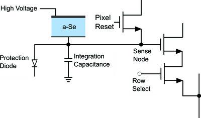
The objective of this work was to fabricate and characterize a new X-ray imaging detector with micrometre-scale pixel dimensions (7.8 µm) and high detection efficiency for hard X-ray energies above 20 keV. A key technology component consists of a monolithic hybrid detector built by direct deposition of an amorphous selenium film on a custom designed CMOS readout integrated circuit. Characterization was carried out at the synchrotron beamline 1-BM-B at the Advanced Photon Source of Argonne National Laboratory. The direct conversion detector demonstrated micrometre-scale spatial resolution with a 63 keV modulation transfer function of 10% at Nyquist frequency. In addition, spatial resolving power down to 8 µm was determined by imaging a transmission bar target at 21 keV. X-ray signal linearity, responsivity and lag were also characterized in the same energy range. Finally, phase contrast edge enhancement was observed in a phase object placed in the beam path. This amorphous selenium/CMOS detector technology can address gaps in commercially available X-ray detectors which limit their usefulness for existing synchrotron applications at energies greater than 50 keV; for example, phase contrast tomography and high-resolution imaging of nanoscale lattice distortions in bulk crystalline materials using Bragg coherent diffraction imaging. The technology will also facilitate the creation of novel synchrotron imaging applications for X-ray energies at or above 20 keV.
中文翻译:

高能微米级像素直接转换X射线探测器
这项工作的目的是制造和表征具有微米级像素尺寸 (7.8 µm) 和对 20 keV 以上硬 X 射线能量的高检测效率的新型 X 射线成像探测器。关键技术组件包括单片混合探测器,该探测器通过在定制设计的 CMOS 读出集成电路上直接沉积非晶硒膜而构建。表征是在阿贡国家实验室先进光子源的同步加速器光束线 1-BM-B 上进行的。直接转换探测器展示了微米级空间分辨率,在奈奎斯特频率下具有 10% 的 63 keV 调制传递函数。此外,低至 8 µm 的空间分辨率是通过对 21 keV 的透射杆目标成像确定的。X射线信号线性度,响应度和滞后也在相同的能量范围内表征。最后,在放置在光束路径中的相位物体中观察到相位对比边缘增强。这种非晶硒/CMOS 探测器技术可以解决商用 X 射线探测器中的缺陷,这些缺陷限制了它们在能量大于 50 keV 的现有同步加速器应用中的有用性;例如,使用布拉格相干衍射成像对块状晶体材料中的纳米级晶格畸变进行相衬断层扫描和高分辨率成像。该技术还将促进为 20 keV 或 20 keV 以上的 X 射线能量创建新型同步加速器成像应用。这种非晶硒/CMOS 探测器技术可以解决商用 X 射线探测器中的缺陷,这些缺陷限制了它们在能量大于 50 keV 的现有同步加速器应用中的有用性;例如,使用布拉格相干衍射成像对块状晶体材料中的纳米级晶格畸变进行相衬断层扫描和高分辨率成像。该技术还将促进为 20 keV 或 20 keV 以上的 X 射线能量创建新型同步加速器成像应用。这种非晶硒/CMOS 探测器技术可以解决商用 X 射线探测器中的缺陷,这些缺陷限制了它们在能量大于 50 keV 的现有同步加速器应用中的有用性;例如,使用布拉格相干衍射成像对块状晶体材料中的纳米级晶格畸变进行相衬断层扫描和高分辨率成像。该技术还将促进为 20 keV 或 20 keV 以上的 X 射线能量创建新型同步加速器成像应用。
更新日期:2021-07-24
中文翻译:
高能微米级像素直接转换X射线探测器
这项工作的目的是制造和表征具有微米级像素尺寸 (7.8 µm) 和对 20 keV 以上硬 X 射线能量的高检测效率的新型 X 射线成像探测器。关键技术组件包括单片混合探测器,该探测器通过在定制设计的 CMOS 读出集成电路上直接沉积非晶硒膜而构建。表征是在阿贡国家实验室先进光子源的同步加速器光束线 1-BM-B 上进行的。直接转换探测器展示了微米级空间分辨率,在奈奎斯特频率下具有 10% 的 63 keV 调制传递函数。此外,低至 8 µm 的空间分辨率是通过对 21 keV 的透射杆目标成像确定的。X射线信号线性度,响应度和滞后也在相同的能量范围内表征。最后,在放置在光束路径中的相位物体中观察到相位对比边缘增强。这种非晶硒/CMOS 探测器技术可以解决商用 X 射线探测器中的缺陷,这些缺陷限制了它们在能量大于 50 keV 的现有同步加速器应用中的有用性;例如,使用布拉格相干衍射成像对块状晶体材料中的纳米级晶格畸变进行相衬断层扫描和高分辨率成像。该技术还将促进为 20 keV 或 20 keV 以上的 X 射线能量创建新型同步加速器成像应用。这种非晶硒/CMOS 探测器技术可以解决商用 X 射线探测器中的缺陷,这些缺陷限制了它们在能量大于 50 keV 的现有同步加速器应用中的有用性;例如,使用布拉格相干衍射成像对块状晶体材料中的纳米级晶格畸变进行相衬断层扫描和高分辨率成像。该技术还将促进为 20 keV 或 20 keV 以上的 X 射线能量创建新型同步加速器成像应用。这种非晶硒/CMOS 探测器技术可以解决商用 X 射线探测器中的缺陷,这些缺陷限制了它们在能量大于 50 keV 的现有同步加速器应用中的有用性;例如,使用布拉格相干衍射成像对块状晶体材料中的纳米级晶格畸变进行相衬断层扫描和高分辨率成像。该技术还将促进为 20 keV 或 20 keV 以上的 X 射线能量创建新型同步加速器成像应用。


 京公网安备 11010802027423号