当前位置:
X-MOL 学术
›
Phys. Status Solidi B
›
论文详情
Our official English website, www.x-mol.net, welcomes your
feedback! (Note: you will need to create a separate account there.)
Impact of Electrical Current on Single GaAs Nanowire Structure
Physica Status Solidi (B) - Basic Solid State Physics ( IF 1.5 ) Pub Date : 2021-05-20 , DOI: 10.1002/pssb.202100056 Danial Bahrami 1 , A. AlHassan 1 , A. Davtyan 1 , R. Zhe 2 , T. Anjum 1 , J. Herranz 3 , L. Geelhaar 3 , D. V. Novikov 4 , R. Timm 2 , Ullrich Pietsch 1
Physica Status Solidi (B) - Basic Solid State Physics ( IF 1.5 ) Pub Date : 2021-05-20 , DOI: 10.1002/pssb.202100056 Danial Bahrami 1 , A. AlHassan 1 , A. Davtyan 1 , R. Zhe 2 , T. Anjum 1 , J. Herranz 3 , L. Geelhaar 3 , D. V. Novikov 4 , R. Timm 2 , Ullrich Pietsch 1
Affiliation
|
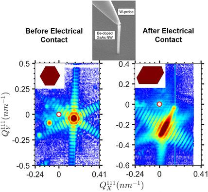
The impact of electrical current on the structure of single free-standing Be-doped GaAs nanowires grown on a Si 111 substrate is investigated. Single nanowires have been structurally analyzed by X-ray nanodiffraction using synchrotron radiation before and after the application of an electrical current. The conductivity measurements on single nanowires in their as-grown geometry have been realized via W-probes installed inside a dual-beam focused ion beam/scanning electron microscopy chamber. Comparing reciprocal space maps of the 111 Bragg reflection, extracted perpendicular to the nanowire growth axis before and after the conductivity measurement, the structural impact of the electrical current is evidenced, including deformation of the hexagonal nanowire cross section, tilting, and bending with respect to the substrate normal. For electrical current densities below 30 A mm−2, the induced changes in the reciprocal space maps are negligible. However, for a current density of 347 A mm−2, the diffraction pattern is completely distorted. The mean cross section of the illuminated nanowire volume is reconstructed from the reciprocal space maps before and after the application of electrical current. Interestingly, the elongation of two pairs of opposing side facets accompanied by shrinkage of the third pair of facets is found. The variations in the nanowire diameter, as well as their tilt and bending, are confirmed by scanning electron microscopy. To explain these findings, material melting due to Joule heating during voltage/current application accompanied by anisotropic deformations induced by the W-probe is suggested.
中文翻译:

电流对单条 GaAs 纳米线结构的影响
研究了电流对在 Si 111 衬底上生长的单根自支撑 Be 掺杂 GaAs 纳米线结构的影响。在施加电流之前和之后,使用同步辐射通过 X 射线纳米衍射对单纳米线进行了结构分析。已通过安装在双束聚焦离子束/扫描电子显微镜室内的 W 探针实现了对生长几何形状的单纳米线的电导率测量。比较在电导率测量之前和之后垂直于纳米线生长轴提取的 111 布拉格反射的倒易空间图,可以证明电流的结构影响,包括六边形纳米线横截面的变形、倾斜和弯曲基材正常。-2,倒易空间图中的诱导变化可以忽略不计。然而,对于347 A mm -2的电流密度,衍射图案完全扭曲。照明纳米线体积的平均横截面是从施加电流之前和之后的倒易空间图重建的。有趣的是,发现了两对相对的侧面的伸长伴随着第三对小面的收缩。纳米线直径的变化以及它们的倾斜和弯曲通过扫描电子显微镜得到证实。为了解释这些发现,建议在电压/电流施加过程中由于焦耳热导致材料熔化,并伴随着 W 探针引起的各向异性变形。
更新日期:2021-05-20
中文翻译:
电流对单条 GaAs 纳米线结构的影响
研究了电流对在 Si 111 衬底上生长的单根自支撑 Be 掺杂 GaAs 纳米线结构的影响。在施加电流之前和之后,使用同步辐射通过 X 射线纳米衍射对单纳米线进行了结构分析。已通过安装在双束聚焦离子束/扫描电子显微镜室内的 W 探针实现了对生长几何形状的单纳米线的电导率测量。比较在电导率测量之前和之后垂直于纳米线生长轴提取的 111 布拉格反射的倒易空间图,可以证明电流的结构影响,包括六边形纳米线横截面的变形、倾斜和弯曲基材正常。-2,倒易空间图中的诱导变化可以忽略不计。然而,对于347 A mm -2的电流密度,衍射图案完全扭曲。照明纳米线体积的平均横截面是从施加电流之前和之后的倒易空间图重建的。有趣的是,发现了两对相对的侧面的伸长伴随着第三对小面的收缩。纳米线直径的变化以及它们的倾斜和弯曲通过扫描电子显微镜得到证实。为了解释这些发现,建议在电压/电流施加过程中由于焦耳热导致材料熔化,并伴随着 W 探针引起的各向异性变形。


 京公网安备 11010802027423号