Microelectronic Engineering ( IF 2.6 ) Pub Date : 2021-05-19 , DOI: 10.1016/j.mee.2021.111572 Chang-Chun Lee , Yu-Min Lin , Hou-Chun Liu , Ji-Yuan Syu , Yuan-Cheng Huang , Tao-Chih Chang
|
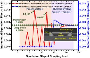
In the development of semiconductor packaging technology from planar to three-dimensional vertical integration, chip interconnection density has increased, and the distance of signal transmission has dropped to improve overall device performance. In this research, an architecture composed of through‑silicon via (TSV) and solder microbump (μbump) is utilized to assemble an ultra thin-type chip into a three-dimensional integrated circuit (3D-IC) package. To explore the influence of residual thermomechanical residual stress induced during the manufacture of the 3D-IC package on the subsequent reliability of the thermal cycling test (TCT), this study establishes a nonlinear simulation methodology for investigating the coupling effect of the manufacturing process and the TCT. The plastic and creep behaviors of the solder μbump are considered in the finite element modeling. The concerned geometric dimensions and underfill materials are also parametrically analyzed. Furthermore, the inelastic strain accumulated in the crucial SnAg solder μbump is examined. Results indicate that the residual strain in the manufacturing process causes an obvious packaging warpage and converges at the subsequent TCT stage. The creep of the solder μbump increases up to 50% in thermal cycling, thereby highlighting the importance of considering the creep model. Moreover, the parameterization of chip thickness can minimize the inelastic strain increment of the solder μbump, and the low Young's modulus of the underfill materials exerts a significant effect on the warpage of the packaging module and the stress compliance of the μbumps.
中文翻译:
在制造过程和温度循环测试的耦合负载作用下,超薄3D-IC封装的可靠性评估
在半导体封装技术从平面垂直集成到三维垂直集成的发展过程中,芯片互连密度提高了,信号传输的距离也缩短了,从而提高了整个器件的性能。在这项研究中,利用由硅通孔(TSV)和焊料微凸点(μbump)组成的体系结构将超薄型芯片组装到三维集成电路(3D-IC)封装中。为了探索在3D-IC封装制造过程中产生的残余热机械残余应力对热循环测试(TCT)后续可靠性的影响,本研究建立了一种非线性仿真方法,以研究制造过程与热电偶的耦合效应。 TCT。在有限元建模中考虑了焊料微凸点的塑性和蠕变行为。还对相关的几何尺寸和底部填充材料进行了参数分析。此外,还检查了在关键SnAg焊料微凸点中累积的非弹性应变。结果表明,制造过程中的残余应变会导致明显的包装翘曲并在随后的TCT阶段收敛。在热循环中,焊锡μbump的蠕变增加高达50%,因此突出了考虑蠕变模型的重要性。此外,芯片厚度的参数化可以最小化焊锡凸块的非弹性应变增量,而底部填充材料的低杨氏模量对封装模块的翘曲和焊锡凸块的应力柔韧性产生重大影响。


 京公网安备 11010802027423号