当前位置:
X-MOL 学术
›
Int. J. Circ. Theory Appl.
›
论文详情
Our official English website, www.x-mol.net, welcomes your
feedback! (Note: you will need to create a separate account there.)
A 4GS/s 8-bit time-interleaved SAR ADC with an energy-efficient architecture in 130 nm CMOS
International Journal of Circuit Theory and Applications ( IF 1.8 ) Pub Date : 2021-05-02 , DOI: 10.1002/cta.3029 Fredy Solis 1 , Álvaro Fernández Bocco 1 , Agustín C. Galetto 1 , Leandro Passetti 1 , Mario R. Hueda 2 , Benjamín T. Reyes 1
International Journal of Circuit Theory and Applications ( IF 1.8 ) Pub Date : 2021-05-02 , DOI: 10.1002/cta.3029 Fredy Solis 1 , Álvaro Fernández Bocco 1 , Agustín C. Galetto 1 , Leandro Passetti 1 , Mario R. Hueda 2 , Benjamín T. Reyes 1
Affiliation
|
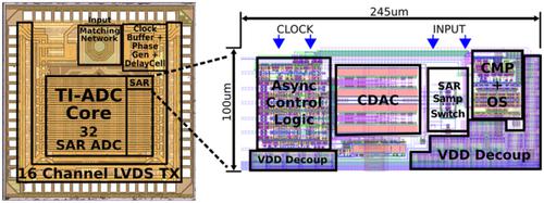
This paper presents the design, implementation, and measurements of a 4 GS/s, 8-bit resolution, time-interleaved (TI) analog-to-digital converter (ADC) comprised of 32 asynchronous successive approximation register (SAR) ADCs. The chip is fabricated in a 130 nm CMOS process. This prototype achieves the highest sampling rate and the best efficiency for a SAR TI-ADC in the process used. An energy-efficient hierarchical T&H architecture, ranked in a 4 × 8 structure, has been used to interleave the aforementioned high number of SAR ADCs avoiding the power hungry buffers typically used in the input signal path and/or T&H outputs. The sampling architecture includes programmable delay cells with up to 104 fs resolution to calibrate sampling time errors. Additionally, the input matching network uses an on-chip inductance to mitigate the impact of the packaging on the analog bandwidth. An efficient SAR ADC implementation is achieved by an optimized comparator design, which allows for both, noise and asynchronous clock control, and includes background DC offset calibration. The test chip is the core of a measurement platform dedicated to the evaluation of mismatch calibration techniques for ADCs used in high speed digital communication systems. To enable this application, a 32Gb/s low-voltage differential signaling interface is included to transmit the samples off-chip without any decimation. The TI-ADC achieves a peak 7.09 effective number of bits (ENOB) (5.47ENOB at Nyquist) and 1.3 GHz input bandwidth with a power consumption of 93 mW at 1.2 V. Each SAR ADC channel achieves a Walden figure of merit (FOM) of 123fJ/conv-step and owing to the efficient interleaved architecture the full TI-ADC achieves a peak FOM of 171fJ/conv-step (526fJ/conv-step at Nyquist).
中文翻译:

采用 130 nm CMOS 节能架构的 4GS/s 8 位时间交错 SAR ADC
本文介绍了由 32 个异步逐次逼近寄存器 (SAR) ADC 组成的 4 GS/s、8 位分辨率、时间交错 (TI) 模数转换器 (ADC) 的设计、实现和测量。该芯片采用 130 nm CMOS 工艺制造。该原型在所使用的工艺中实现了 SAR TI-ADC 的最高采样率和最佳效率。一种采用 4 × 8 结构的节能分层 T&H 架构已被用于交错上述大量 SAR ADC,从而避免了通常用于输入信号路径和/或 T&H 输出中的耗电缓冲器。采样架构包括具有高达 104 fs 分辨率的可编程延迟单元,用于校准采样时间误差。此外,输入匹配网络使用片上电感来减轻封装对模拟带宽的影响。高效的 SAR ADC 实现是通过优化的比较器设计实现的,该设计允许噪声和异步时钟控制,并包括背景 DC 偏移校准。测试芯片是测量平台的核心,专门用于评估高速数字通信系统中使用的 ADC 的失配校准技术。为支持此应用,包含一个 32Gb/s 低压差分信号接口,用于在片外传输样本而无需任何抽取。TI-ADC 实现了峰值 7.09 有效位数 (ENOB)(奈奎斯特时为 5.47ENOB)和 1.3 GHz 输入带宽,在 1.2 V 时功耗为 93 mW。
更新日期:2021-05-02
中文翻译:
采用 130 nm CMOS 节能架构的 4GS/s 8 位时间交错 SAR ADC
本文介绍了由 32 个异步逐次逼近寄存器 (SAR) ADC 组成的 4 GS/s、8 位分辨率、时间交错 (TI) 模数转换器 (ADC) 的设计、实现和测量。该芯片采用 130 nm CMOS 工艺制造。该原型在所使用的工艺中实现了 SAR TI-ADC 的最高采样率和最佳效率。一种采用 4 × 8 结构的节能分层 T&H 架构已被用于交错上述大量 SAR ADC,从而避免了通常用于输入信号路径和/或 T&H 输出中的耗电缓冲器。采样架构包括具有高达 104 fs 分辨率的可编程延迟单元,用于校准采样时间误差。此外,输入匹配网络使用片上电感来减轻封装对模拟带宽的影响。高效的 SAR ADC 实现是通过优化的比较器设计实现的,该设计允许噪声和异步时钟控制,并包括背景 DC 偏移校准。测试芯片是测量平台的核心,专门用于评估高速数字通信系统中使用的 ADC 的失配校准技术。为支持此应用,包含一个 32Gb/s 低压差分信号接口,用于在片外传输样本而无需任何抽取。TI-ADC 实现了峰值 7.09 有效位数 (ENOB)(奈奎斯特时为 5.47ENOB)和 1.3 GHz 输入带宽,在 1.2 V 时功耗为 93 mW。


 京公网安备 11010802027423号