Our official English website, www.x-mol.net, welcomes your
feedback! (Note: you will need to create a separate account there.)
Steep-Slope Gate-Connected Atomic Threshold Switching Field-Effect Transistor with MoS2 Channel and Its Application to Infrared Detectable Phototransistors
Advanced Science ( IF 14.3 ) Pub Date : 2021-05-03 , DOI: 10.1002/advs.202100208 Seung-Geun Kim 1 , Seung-Hwan Kim 2 , Gwang-Sik Kim 2 , Hyeok Jeon 1 , Taehyun Kim 1 , Hyun-Yong Yu 2
Advanced Science ( IF 14.3 ) Pub Date : 2021-05-03 , DOI: 10.1002/advs.202100208 Seung-Geun Kim 1 , Seung-Hwan Kim 2 , Gwang-Sik Kim 2 , Hyeok Jeon 1 , Taehyun Kim 1 , Hyun-Yong Yu 2
Affiliation
|
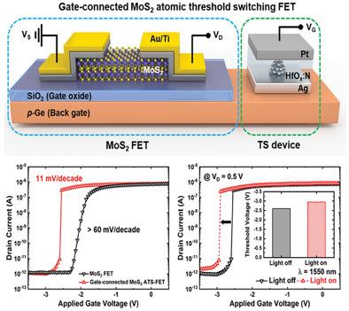
For next-generation electronics and optoelectronics, 2D-layered nanomaterial-based field effect transistors (FETs) have garnered attention as promising candidates owing to their remarkable properties. However, their subthreshold swings (SS) cannot be lower than 60 mV/decade owing to the limitation of the thermionic carrier injection mechanism, and it remains a major challenge in 2D-layered nanomaterial-based transistors. Here, a gate-connected MoS2 atomic threshold switching FET using a nitrogen-doped HfO2-based threshold switching (TS) device is developed. The proposed device achieves an extremely low SS of 11 mV/decade and a high on-off ratio of ≈106 by maintaining a high on-state drive current due to the steep switching of the TS device at the gate region. In particular, the proposed device can function as an infrared detectable phototransistor with excellent optical properties. The proposed device is expected to pave the way for the development of future 2D channel-based electrical and optical transistors.
中文翻译:

MoS2通道的陡坡门连接原子阈值开关场效应晶体管及其在红外探测光电晶体管中的应用
对于下一代电子学和光电子学,基于二维层状纳米材料的场效应晶体管(FET)因其卓越的性能而作为有前途的候选者而受到关注。然而,由于热电子载流子注入机制的限制,它们的亚阈值摆幅(SS)不能低于60 mV/decade,这仍然是基于二维层状纳米材料的晶体管的主要挑战。这里,开发了一种使用氮掺杂HfO 2基阈值开关(TS)器件的栅极连接的MoS 2原子阈值开关FET。由于 TS 器件在栅极区域的陡峭开关,所提出的器件通过保持高导通状态驱动电流,实现了 11 mV/十倍频程的极低SS和约 10 6的高开关比。特别是,所提出的器件可以用作具有优异光学特性的红外可检测光电晶体管。所提出的器件预计将为未来基于二维通道的电气和光学晶体管的开发铺平道路。
更新日期:2021-06-24
中文翻译:
MoS2通道的陡坡门连接原子阈值开关场效应晶体管及其在红外探测光电晶体管中的应用
对于下一代电子学和光电子学,基于二维层状纳米材料的场效应晶体管(FET)因其卓越的性能而作为有前途的候选者而受到关注。然而,由于热电子载流子注入机制的限制,它们的亚阈值摆幅(SS)不能低于60 mV/decade,这仍然是基于二维层状纳米材料的晶体管的主要挑战。这里,开发了一种使用氮掺杂HfO 2基阈值开关(TS)器件的栅极连接的MoS 2原子阈值开关FET。由于 TS 器件在栅极区域的陡峭开关,所提出的器件通过保持高导通状态驱动电流,实现了 11 mV/十倍频程的极低SS和约 10 6的高开关比。特别是,所提出的器件可以用作具有优异光学特性的红外可检测光电晶体管。所提出的器件预计将为未来基于二维通道的电气和光学晶体管的开发铺平道路。


 京公网安备 11010802027423号