Microelectronic Engineering ( IF 2.3 ) Pub Date : 2021-05-04 , DOI: 10.1016/j.mee.2021.111560 Peng Chen , Lei Wu , Jian Gao , Chengqiang Feng , Bingjun Yu , Linmao Qian
|
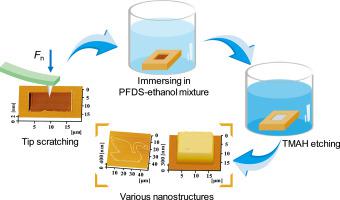
A self-assembled 1H,1H,2H,2H-perfluorodecyltriethoxysilane (PFDS) film was prepared on a diamond tip scratched silicon surface, and presented stronger anti-etching ability during subsequent selective etching than direct scratch mask. The effect of self-assembly time, normal load in scratching and etching time on anti-etching performance of the PFDS film were investigated by comparing the height and topography of fabricated mesas. It was found that the self-assembly of 2 h was enough for the formation of PFDS film, and the increase of normal load in scratching could improve anti-etching ability of the film. The result of X-ray photoelectron spectroscopy (XPS) suggested that PFDS molecules were selectively adsorbed on scratched silicon surface. This study provides a novel route for site-controlled formation of self-assembled mask and helps produce higher nanostructures in selective etching, which is promising for constructing functionalized micro/nano devices.
中文翻译:
改进的基于扫描探针的光刻技术:现场控制形成自组装膜作为蚀刻掩模
在金刚石尖端划痕的硅表面上制备了自组装的1H,1H,2H,2H-全氟癸基三乙氧基硅烷(PFDS)膜,与直接划痕掩模相比,该膜在随后的选择性蚀刻过程中具有更强的抗蚀刻能力。通过比较制备的台面的高度和形貌,研究了自组装时间,刮擦的正常载荷和蚀刻时间对PFDS膜抗蚀刻性能的影响。发现2小时的自组装足以形成PFDS膜,并且增加刮擦的正常载荷可以提高膜的抗蚀刻能力。X射线光电子能谱(XPS)的结果表明,PFDS分子被选择性地吸附在划痕的硅表面上。


 京公网安备 11010802027423号