当前位置:
X-MOL 学术
›
Phys. Status Solidi. Rapid Res. Lett.
›
论文详情
Our official English website, www.x-mol.net, welcomes your
feedback! (Note: you will need to create a separate account there.)
A Synaptic Transistor Based on Monolayer Monocrystalline-MoS2 for Neuromorphic Applications
Physica Status Solidi-Rapid Research Letters ( IF 2.5 ) Pub Date : 2021-04-30 , DOI: 10.1002/pssr.202100007 Meng Yan 1 , Kai Hu 1 , Fang Wang 1 , Xin Shan 1 , Xin Lin 1 , Peng Chen 1 , Xuanyu Zhao 1 , Junqing Wei 2 , Zhitang Song 3 , Kailiang Zhang 1
Physica Status Solidi-Rapid Research Letters ( IF 2.5 ) Pub Date : 2021-04-30 , DOI: 10.1002/pssr.202100007 Meng Yan 1 , Kai Hu 1 , Fang Wang 1 , Xin Shan 1 , Xin Lin 1 , Peng Chen 1 , Xuanyu Zhao 1 , Junqing Wei 2 , Zhitang Song 3 , Kailiang Zhang 1
Affiliation
|
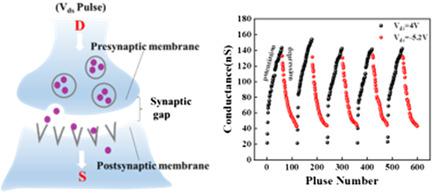
Ultrathin 2D semiconductor materials have attracted tremendous attention due to their potential application in neuromorphic computing, especially for electronic devices with high stability and low energy consumption. Two-terminal memristors cannot extend the range of functionalities for complex neuromorphic applications due to their inherent single presynaptic input; thus three-terminal synaptic transistors based on monolayer monocrystalline-MoS2 films grown by chemical vapor deposition (CVD) are fabricated in this work. Importantly, there are two modes including drain and gate dual tunability available in nonvolatile memory functions. Both drain terminal and gate terminal can be used as presynaptic inputs to successfully simulate excitatory/inhibitory postsynaptic current (EPSC/IPSC), spike-amplitude-dependent plasticity (SADP), spike-timing-dependent plasticity (STDP), and long-term plasticity (LTP) of biological synapses, providing multiple degrees of freedom for synaptic weight modulation. The conductance modulation of drain and gate terminals can be attributed to the migration and charges trapping/detrapping process of sulfur vacancies. Using monocrystalline-MoS2 films, the device not only attains a lower operation voltage and a higher endurance (5000 cycles), but exhibit low energy consumption during the LTP process (≈3.75 pJ) with the gate terminal, indicating more flexibility and great potential of complex neuromorphic application.
中文翻译:

用于神经形态应用的基于单层单晶-MoS2 的突触晶体管
超薄二维半导体材料由于其在神经形态计算中的潜在应用而引起了极大的关注,特别是对于具有高稳定性和低能耗的电子设备。由于其固有的单一突触前输入,两端忆阻器无法扩展复杂神经形态应用的功能范围;因此,基于单层单晶-MoS 2 的三端突触晶体管在这项工作中制造了通过化学气相沉积 (CVD) 生长的薄膜。重要的是,非易失性存储器功能中有两种模式,包括漏极和栅极双重可调性。漏极端子和栅极端子均可用作突触前输入,以成功模拟兴奋性/抑制性突触后电流 (EPSC/IPSC)、尖峰幅度依赖性可塑性 (SADP)、尖峰时间依赖性可塑性 (STDP) 和长期生物突触的可塑性 (LTP),为突触权重调节提供多个自由度。漏极和栅极端子的电导调制可归因于硫空位的迁移和电荷捕获/释放过程。使用单晶-MoS 2 薄膜,该器件不仅获得了更低的工作电压和更高的耐久性(5000 次循环),而且在 LTP 过程中表现出低能耗(≈3.75 pJ)与栅极终端,表明复杂的神经形态应用具有更大的灵活性和巨大潜力。
更新日期:2021-04-30
中文翻译:
用于神经形态应用的基于单层单晶-MoS2 的突触晶体管
超薄二维半导体材料由于其在神经形态计算中的潜在应用而引起了极大的关注,特别是对于具有高稳定性和低能耗的电子设备。由于其固有的单一突触前输入,两端忆阻器无法扩展复杂神经形态应用的功能范围;因此,基于单层单晶-MoS 2 的三端突触晶体管在这项工作中制造了通过化学气相沉积 (CVD) 生长的薄膜。重要的是,非易失性存储器功能中有两种模式,包括漏极和栅极双重可调性。漏极端子和栅极端子均可用作突触前输入,以成功模拟兴奋性/抑制性突触后电流 (EPSC/IPSC)、尖峰幅度依赖性可塑性 (SADP)、尖峰时间依赖性可塑性 (STDP) 和长期生物突触的可塑性 (LTP),为突触权重调节提供多个自由度。漏极和栅极端子的电导调制可归因于硫空位的迁移和电荷捕获/释放过程。使用单晶-MoS 2 薄膜,该器件不仅获得了更低的工作电压和更高的耐久性(5000 次循环),而且在 LTP 过程中表现出低能耗(≈3.75 pJ)与栅极终端,表明复杂的神经形态应用具有更大的灵活性和巨大潜力。


 京公网安备 11010802027423号