当前位置:
X-MOL 学术
›
Phys. Status Solidi B
›
论文详情
Our official English website, www.x-mol.net, welcomes your
feedback! (Note: you will need to create a separate account there.)
First-Principles Study of the Effects of Interstitial H and Point Vacancies on the p-Type of Conductive Properties of Be/Mg/Ca-Doped GaN
Physica Status Solidi (B) - Basic Solid State Physics ( IF 1.5 ) Pub Date : 2021-04-28 , DOI: 10.1002/pssb.202100023 Xiang Yin 1 , Qingyu Hou 1, 2 , Hao Chen 1
Physica Status Solidi (B) - Basic Solid State Physics ( IF 1.5 ) Pub Date : 2021-04-28 , DOI: 10.1002/pssb.202100023 Xiang Yin 1 , Qingyu Hou 1, 2 , Hao Chen 1
Affiliation
|
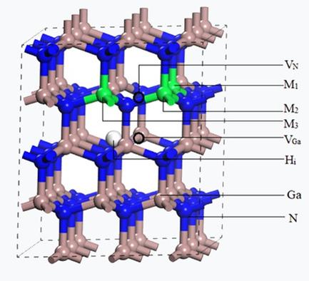
Obtaining a reliable positive-type (p-type) GaN semiconductor is difficult because of the unipolarity of GaN. This difficulty is one of the bottlenecks restricting the development of GaN-based optoelectronic devices. To address this problem, this paper adopted the method of generalized gradient approximation (GGA) plane wave ultrasoft pseudopotential based on the framework of density functional theory to construct Ga35MN36, Ga34MN36, and Ga34MHiN36 (M = Be/Mg/Ca; Hi = interstitial hydrogen) models. Ga35MN35 and Ga35MHiN35 (M = Be/Mg/Ca) models were also constructed. Results of our calculations indicated that the Ga35MN35 and Ga35MHiN35 (M = Be/Mg/Ca) models cannot achieve a p-type doping system. Furthermore, the formation energy of Ga34MN36 and Ga34MHiN36 (M = Be/Mg/Ca) systems was greater under Ga-rich conditions than that under N-rich conditions, indicating that both doping systems more readily formed and had a more stable structure under N-rich conditions. Moreover, the formation energy of Ga34MHiN36 (M = Be/Mg/Ca) system was lower than that of Ga34MN36 (M = Be/Mg/Ca) system, and the existence of interstitial H proved to be beneficial to the improvement in system stability. The Ga34CaHiN36 system had the largest hole mobility and the best conductivity. Therefore, the Ga34CaHiN36 system is an ideal material for the application of conductive GaN devices. This study provides guidance into the preparation of p-type conductive GaN materials.
中文翻译:

间隙 H 和点空位对 Be/Mg/Ca 掺杂 GaN p 型导电性能影响的第一性原理研究
由于 GaN 的单极性,因此很难获得可靠的正型(p 型)GaN 半导体。这一难点是制约GaN基光电器件发展的瓶颈之一。针对这一问题,本文基于密度泛函理论的框架,采用广义梯度逼近(GGA)平面波超软赝势的方法构造了Ga 35 MN 36、Ga 34 MN 36和Ga 34 MH i N 36 (M = Be/Mg/Ca;H i = 间隙氢)模型。Ga 35 MN 35和 Ga 35 MH i N还构建了35 (M = Be/Mg/Ca) 模型。我们的计算结果表明 Ga 35 MN 35和 Ga 35 MH i N 35 (M = Be/Mg/Ca) 模型无法实现 p 型掺杂系统。此外,Ga 34 MN 36和Ga 34 MH i N 36 (M = Be/Mg/Ca)体系在富Ga条件下的形成能大于富N条件下的形成能,表明两种掺杂体系更容易形成并且在富氮条件下具有更稳定的结构。此外,Ga 34 MH i N 36的形成能(M = Be/Mg/Ca)体系低于Ga 34 MN 36 (M = Be/Mg/Ca)体系,且间隙H的存在被证明有利于提高体系稳定性。Ga 34 CaH i N 36体系具有最大的空穴迁移率和最好的导电性。因此,Ga 34 CaH i N 36体系是应用导电GaN器件的理想材料。该研究为 p 型导电 GaN 材料的制备提供了指导。
更新日期:2021-04-28
中文翻译:
间隙 H 和点空位对 Be/Mg/Ca 掺杂 GaN p 型导电性能影响的第一性原理研究
由于 GaN 的单极性,因此很难获得可靠的正型(p 型)GaN 半导体。这一难点是制约GaN基光电器件发展的瓶颈之一。针对这一问题,本文基于密度泛函理论的框架,采用广义梯度逼近(GGA)平面波超软赝势的方法构造了Ga 35 MN 36、Ga 34 MN 36和Ga 34 MH i N 36 (M = Be/Mg/Ca;H i = 间隙氢)模型。Ga 35 MN 35和 Ga 35 MH i N还构建了35 (M = Be/Mg/Ca) 模型。我们的计算结果表明 Ga 35 MN 35和 Ga 35 MH i N 35 (M = Be/Mg/Ca) 模型无法实现 p 型掺杂系统。此外,Ga 34 MN 36和Ga 34 MH i N 36 (M = Be/Mg/Ca)体系在富Ga条件下的形成能大于富N条件下的形成能,表明两种掺杂体系更容易形成并且在富氮条件下具有更稳定的结构。此外,Ga 34 MH i N 36的形成能(M = Be/Mg/Ca)体系低于Ga 34 MN 36 (M = Be/Mg/Ca)体系,且间隙H的存在被证明有利于提高体系稳定性。Ga 34 CaH i N 36体系具有最大的空穴迁移率和最好的导电性。因此,Ga 34 CaH i N 36体系是应用导电GaN器件的理想材料。该研究为 p 型导电 GaN 材料的制备提供了指导。


 京公网安备 11010802027423号