当前位置:
X-MOL 学术
›
Int. J. Circ. Theory Appl.
›
论文详情
Our official English website, www.x-mol.net, welcomes your
feedback! (Note: you will need to create a separate account there.)
Analysis and design of ultra-wideband low noise amplifier using complementary structure with series inductive peaking technique and shunt feedback
International Journal of Circuit Theory and Applications ( IF 1.8 ) Pub Date : 2021-04-27 , DOI: 10.1002/cta.3039 Amir Hossein Kazemi 1 , Mohsen Hayati 1
International Journal of Circuit Theory and Applications ( IF 1.8 ) Pub Date : 2021-04-27 , DOI: 10.1002/cta.3039 Amir Hossein Kazemi 1 , Mohsen Hayati 1
Affiliation
|
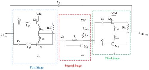
In this paper, an ultra-wideband low noise amplifier (LNA) is presented using 0.18-μm RF CMOS technology. A complementary structure with series inductive peaking technique is introduced by using two inductor-loops to achieve flat gain. In the first and third stages, two complementary structures are utilized to achieve a high and flat gain, a wideband input impedance matching and a low noise figure. In addition, a shunt feedback is utilized to increase input impedance matching and stability. In the second stage, a common source structure is used as interstage, which increases the −3 dB bandwidth. The designed LNA presents a high and flat gain of 15.6–16.5 dB, an excellent input return loss better than −11 dB and a good NF of 2.2–3 dB in the frequency range of 3.1–10.6 GHz. Also, the proposed structure consumes 6.8 mW from a 0.8-V supply voltage and has an IIP3 of −4 dBm at 6.5 GHz. The proposed structure only occupies 0.59 mm2.
中文翻译:

串联电感峰值技术和并联反馈互补结构的超宽带低噪声放大器分析与设计
在本文中,提出了一种使用 0.18-μm RF CMOS 技术的超宽带低噪声放大器 (LNA)。通过使用两个电感回路来实现平坦增益,引入了具有串联电感峰值技术的互补结构。在第一和第三阶段,利用两个互补结构来实现高且平坦的增益、宽带输入阻抗匹配和低噪声系数。此外,还利用分流反馈来增加输入阻抗匹配和稳定性。在第二阶段,公共源结构用作级间,这增加了 -3 dB 带宽。设计的 LNA 具有 15.6–16.5 dB 的高且平坦的增益、优于 −11 dB 的出色输入回波损耗以及 3.1–10.6 GHz 频率范围内 2.2–3 dB 的良好 NF。此外,所提出的结构从 0.8 mW 消耗 6.8 mW。8V 电源电压,并且在 6.5 GHz 时具有 -4 dBm 的 IIP3。建议的结构仅占用 0.59 mm2 .
更新日期:2021-04-27
中文翻译:
串联电感峰值技术和并联反馈互补结构的超宽带低噪声放大器分析与设计
在本文中,提出了一种使用 0.18-μm RF CMOS 技术的超宽带低噪声放大器 (LNA)。通过使用两个电感回路来实现平坦增益,引入了具有串联电感峰值技术的互补结构。在第一和第三阶段,利用两个互补结构来实现高且平坦的增益、宽带输入阻抗匹配和低噪声系数。此外,还利用分流反馈来增加输入阻抗匹配和稳定性。在第二阶段,公共源结构用作级间,这增加了 -3 dB 带宽。设计的 LNA 具有 15.6–16.5 dB 的高且平坦的增益、优于 −11 dB 的出色输入回波损耗以及 3.1–10.6 GHz 频率范围内 2.2–3 dB 的良好 NF。此外,所提出的结构从 0.8 mW 消耗 6.8 mW。8V 电源电压,并且在 6.5 GHz 时具有 -4 dBm 的 IIP3。建议的结构仅占用 0.59 mm2 .


 京公网安备 11010802027423号