Surfaces and Interfaces ( IF 5.7 ) Pub Date : 2021-04-20 , DOI: 10.1016/j.surfin.2021.101131 Vishakha Kaushik , Mujeeb Ahmad , Pintu Das , B.R. Mehta
|
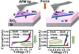
In the present study, AFM metal tip induced loading force dependent electrical transport behaviour of WS2 domains synthesized using chemical vapour deposition technique has been investigated. Raman spectroscopy, optical microscopy and atomic force microscopy (AFM) techniques have been employed to characterize the synthesized two-dimensional (2D) domains. The local nanoscale I-V measurements have been carried out as a function of loading force (53 – 300 nN) using conductive atomic force microscopy to probe the interface formed between AFM tip (Pt coated) and 2D domains of WS2 layers. An interesting phenomena of decreasing junction current with increasing loading force obtained at the centre of single layer WS2 sample is opposed by an increasing junction current at the edges of domain. Loading force induced spatially varying, compressive and tensile strain resulting in charge polarization causing an opposite flow of majority electron carriers away and towards the tip-WS2 domain has been explained as the possible mechanism for the applied opposing uniaxial strains. This study reports the influence of single layer nature of WS2 constituting polar edges and wrinkle terminations on electronic properties of metal-semiconductor contacts. These results are crucial for understanding the junction properties and application of 2D material based devices in next-generation electronics.
中文翻译:
了解2D性质在WS 2层中的接合点属性中的作用;AFM尖端产生的加载力对空间变化接触的影响
在本研究中,已经研究了AFM金属尖端诱导的负载力,该负载依赖于使用化学气相沉积技术合成的WS 2域的电传输行为。拉曼光谱,光学显微镜和原子力显微镜(AFM)技术已被用来表征合成的二维(2D)域。局部纳米级IV测量是根据加载力(53 – 300 nN)进行的,使用导电原子力显微镜来探测AFM尖端(Pt涂层)和WS 2层的2D域之间形成的界面。随着在单层WS 2中心获得的增加的加载力,结电流减小的有趣现象样品被畴边缘的结电流增加所抵消。加载力引起的空间变化,压缩和拉伸应变会导致电荷极化,从而导致大多数电子载流子反向流动并流向尖端WS 2域,这已被解释为施加反向单轴应变的可能机理。这项研究报告了构成极性边缘和皱纹终端的WS 2的单层性质对金属-半导体触点的电子性能的影响。这些结果对于理解结点特性以及基于2D材料的设备在下一代电子产品中的应用至关重要。


 京公网安备 11010802027423号