当前位置:
X-MOL 学术
›
Phys. Rev. Materials
›
论文详情
Our official English website, www.x-mol.net, welcomes your
feedback! (Note: you will need to create a separate account there.)
Valley relaxation of resident electrons and holes in a monolayer semiconductor: Dependence on carrier density and the role of substrate-induced disorder
Physical Review Materials ( IF 3.1 ) Pub Date : 2021-04-05 , DOI: 10.1103/physrevmaterials.5.044001 Jing Li , M. Goryca , K. Yumigeta , H. Li , S. Tongay , S. A. Crooker
Physical Review Materials ( IF 3.1 ) Pub Date : 2021-04-05 , DOI: 10.1103/physrevmaterials.5.044001 Jing Li , M. Goryca , K. Yumigeta , H. Li , S. Tongay , S. A. Crooker
|
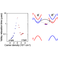
Using time-resolved optical Kerr rotation, we measure the low-temperature valley dynamics of resident electrons and holes in exfoliated monolayers as a systematic function of carrier density. In an effort to reconcile the many disparate timescales of carrier valley dynamics in monolayer semiconductors reported to date, we directly compare the doping-dependent valley relaxation in two electrostatically gated monolayers having different dielectric environments. In a fully encapsulated structure (, where hBN is hexagonal boron nitride), valley relaxation is found to be monoexponential. The valley relaxation time is quite long at low carrier densities, but decreases rapidly to less than 100 ns at high electron or hole densities . In contrast, in a partially encapsulated monolayer placed directly on silicon dioxide , carrier valley relaxation is multiexponential at low carrier densities. The difference is attributed to environmental disorder from the substrate. Unexpectedly, very small out-of-plane magnetic fields can increase , especially in the structure, suggesting that localized states induced by disorder can play an important role in depolarizing spins and mediating the valley relaxation of resident carriers in monolayer transition-metal dichalcogenide semiconductors.
中文翻译:

单层半导体中驻留电子和空穴的谷弛豫:取决于载流子密度和衬底诱导的无序作用
使用时间分辨光学Kerr旋转,我们测量了脱落的电子和空穴的低温谷动态 单层作为载流子密度的系统函数。为了调和迄今为止报道的单层半导体中载流子谷动态的许多不同时间尺度,我们直接比较了两个静电门控中掺杂相关的谷弛豫具有不同介电环境的单层。在完全封装的结构中(,其中hBN是六方氮化硼),发现山谷弛豫是单指数的。山谷放松时间 很长 在低载流子密度下,但在高电子或空穴密度下迅速下降到小于100 ns 。相反,在部分封装的情况下 单层直接放置在二氧化硅上 在低载流子密度下,载流子谷弛豫是多指数的。差异归因于来自基质。出乎意料的是,非常小的面外磁场会增加,尤其是在 这种结构表明,由无序引起的局部状态可以在使自旋去极化并介导单层过渡金属二卤化半导体中常驻载流子的谷弛豫中起重要作用。
更新日期:2021-04-05
中文翻译:
单层半导体中驻留电子和空穴的谷弛豫:取决于载流子密度和衬底诱导的无序作用
使用时间分辨光学Kerr旋转,我们测量了脱落的电子和空穴的低温谷动态 单层作为载流子密度的系统函数。为了调和迄今为止报道的单层半导体中载流子谷动态的许多不同时间尺度,我们直接比较了两个静电门控中掺杂相关的谷弛豫具有不同介电环境的单层。在完全封装的结构中(,其中hBN是六方氮化硼),发现山谷弛豫是单指数的。山谷放松时间 很长 在低载流子密度下,但在高电子或空穴密度下迅速下降到小于100 ns 。相反,在部分封装的情况下 单层直接放置在二氧化硅上 在低载流子密度下,载流子谷弛豫是多指数的。差异归因于来自基质。出乎意料的是,非常小的面外磁场会增加,尤其是在 这种结构表明,由无序引起的局部状态可以在使自旋去极化并介导单层过渡金属二卤化半导体中常驻载流子的谷弛豫中起重要作用。


 京公网安备 11010802027423号