当前位置:
X-MOL 学术
›
Adv. Theory Simul.
›
论文详情
Our official English website, www.x-mol.net, welcomes your
feedback! (Note: you will need to create a separate account there.)
Layer‐Controlled Low‐Power Tunneling Transistors Based on SnS Homojunction
Advanced Theory and Simulations ( IF 2.9 ) Pub Date : 2021-04-02 , DOI: 10.1002/adts.202000290 Jiakun Liang 1 , Hong Li 1 , Fengbin Liu 1 , Jing Lu 2, 3, 4
Advanced Theory and Simulations ( IF 2.9 ) Pub Date : 2021-04-02 , DOI: 10.1002/adts.202000290 Jiakun Liang 1 , Hong Li 1 , Fengbin Liu 1 , Jing Lu 2, 3, 4
Affiliation
|
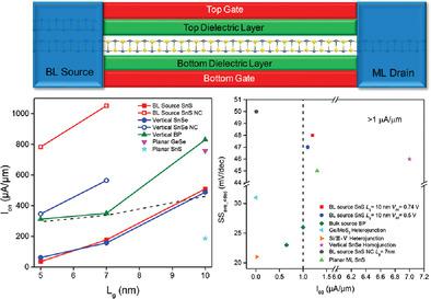
Utilizing the layer‐controlled bandgap of a 2D material is an effective way of improving a tunneling field‐effect transistor (TFET) device's performance because of the narrowing tunneling barrier. An ab initio quantum transport method is used to study the SnS homojunction TFETs at a sub‐10 nm scale through layer controlling. The optimal SnS homojunction TFET has a bilayer SnS as the source electrode, which possesses a low leakage current like the ML SnS TFET and a high on‐state current like the BL SnS TFET. The low SSave_4dec (subthreshold swing over four decades of the drain currents) of ≈47–48 mV dec−1 and I60 (drain current at 60 mV dec−1) of ≈1.1–1.2 µA µm−1 implies the BL source SnS TFET, a fast low‐power (LP) device. The optimal BL source SnS TFET with a gate length of Lg = 10 nm exceeds the LP device requirement of the International Technology Roadmap for Semiconductors (ITRS) (2013 version), and its negative capacitance counterparts can exceed the ITRS 2028 target for LP device at Lg = 5 nm.
中文翻译:

基于SnS同质结的层控制低功率隧穿晶体管
由于隧穿势垒变窄,利用2D材料的层控制带隙是提高隧穿场效应晶体管(TFET)器件性能的有效方法。从头开始量子传输方法用于通过层控制研究小于10 nm规模的SnS同质结TFET。最佳的SnS同质结TFET以双层SnS作为源极,像ML SnS TFET一样具有低泄漏电流,而像BL SnS TFET一样具有高导通电流。低的SS ave_4dec(漏极电流的四个阈值摆幅)约为≈47-48mV dec -1,I 60(约为60 mV dec -1时的漏极电流)约为1.1-1.2 µA µm -1意味着BL源SnS TFET是一种快速的低功耗(LP)器件。栅极长度为L g = 10 nm的最佳BL源SnS TFET超过了国际半导体技术路线图(ITRS)(2013版)的LP器件要求,其负电容可以超过LP器件的ITRS 2028目标在L g = 5 nm处。
更新日期:2021-05-05
中文翻译:
基于SnS同质结的层控制低功率隧穿晶体管
由于隧穿势垒变窄,利用2D材料的层控制带隙是提高隧穿场效应晶体管(TFET)器件性能的有效方法。从头开始量子传输方法用于通过层控制研究小于10 nm规模的SnS同质结TFET。最佳的SnS同质结TFET以双层SnS作为源极,像ML SnS TFET一样具有低泄漏电流,而像BL SnS TFET一样具有高导通电流。低的SS ave_4dec(漏极电流的四个阈值摆幅)约为≈47-48mV dec -1,I 60(约为60 mV dec -1时的漏极电流)约为1.1-1.2 µA µm -1意味着BL源SnS TFET是一种快速的低功耗(LP)器件。栅极长度为L g = 10 nm的最佳BL源SnS TFET超过了国际半导体技术路线图(ITRS)(2013版)的LP器件要求,其负电容可以超过LP器件的ITRS 2028目标在L g = 5 nm处。


 京公网安备 11010802027423号