Microelectronics Reliability ( IF 1.6 ) Pub Date : 2021-03-02 , DOI: 10.1016/j.microrel.2021.114068 Mostafa AbdelAziz , Di Erick Xu , Guotao Wang , Michael Mayer
|
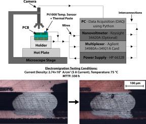
With the increasing demands and consequent miniaturization of electronic devices, electromigration is posing a challenge to the reliability not only of integrated circuits but also of the electronic packages. We report a methodology that allows for quasi-continuous in-situ optical microscopic imaging of a cross-sectioned solder joint (sample) during testing for electromigration. A SAC305 solder joint in a flip configuration was coated in epoxy and cross-sectioned. Current stressing was applied to producing electromigration, with a theoretical current density of 1.37 × 10⁴ A/cm2 for 5 A of current. In-situ optical microscopic imaging and resistance measurements were performed simultaneously until an open circuit was observed.
A crack and void started to form in an example experiment, and their evolution was recorded using the real-time imaging. The void and the crack continued growing until the end of current stressing. The void area at the cross-section grew to 1500 μm2 while the crack grew to a length of 110 μm. After 330 h, the experiment was stopped as an open circuit occurred, which was preceded by a 10% rise of the resistance, indicating failure due to electromigration. During the end of the test, the test vehicle temperature increased by 20 °C as a result of increased Joule heating due to the loss in cross-sectional area of the solder joint. The location of the void did not agree with the expected current crowding location at the solder joint corner. It was inferred that the formation of cracks due to internal stresses prompted the formation of the void at that location that resulted in the open circuit, demonstrating the interconnection between the various failure mechanisms caused by EM. Microstructural changes were also monitored after the open circuit and were possibly due to the thermal stress occurring once the sample cooled down. Hillock formation and additional cracks were observed 30 min after the open circuit. The results highlight the unique capacity of real-time imaging to support more detailed electromigration research in solder joints by tracing the source of specific failure events.
中文翻译:
焊点中的电迁移:用于实时观察的横截面模型系统
随着电子设备的需求增加和随之而来的小型化,电迁移不仅对集成电路的可靠性而且对电子封装的可靠性提出了挑战。我们报告了一种方法,该方法可在电迁移测试期间对横截面焊点(样品)进行准连续原位光学显微成像。翻转配置的SAC305焊点涂有环氧树脂并进行了横截面处理。施加电流应力以产生电迁移,对于5 A电流,理论电流密度为1.37×10 4 A / cm 2。同时进行原位光学显微镜成像和电阻测量,直到观察到断路为止。
在示例实验中开始形成裂缝和空隙,并使用实时成像记录了它们的演变。空隙和裂纹持续增长,直到电流应力结束。在横截面中的空隙面积增长至1500μm 2而裂纹扩展到110μm的长度。330小时后,由于发生开路而停止了实验,在此之前电阻增加了10%,这表明由于电迁移而导致的故障。在测试结束时,由于焊点截面积的损失,焦耳热增加,导致测试车辆温度升高了20°C。空洞的位置与焊点拐角处的预期电流拥挤位置不一致。据推测,由于内部应力而导致的裂纹的形成促使在该位置处形成空隙,从而导致开路,证明了由EM引起的各种失效机制之间的相互联系。断路后也监测了微观结构的变化,这可能是由于样品冷却后发生的热应力。开路后30分钟观察到小丘形成和另外的裂缝。结果突出了实时成像的独特能力,可通过跟踪特定故障事件的来源来支持更详细的焊点电迁移研究。


 京公网安备 11010802027423号