Optik Pub Date : 2021-03-01 , DOI: 10.1016/j.ijleo.2021.166629 M.A. Mora-Ramírez , M. Chávez Portillo , A. Reyes Díaz , O. Portillo Moreno
|
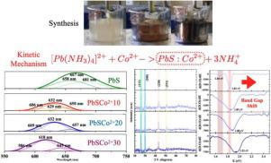
We present theoretical and experimental results in PbS nanocrystalline thin films systematically doped with Co2+ ions utilizing the green Chemical Bath Deposition technique at ∼90 °C. All growth parameters are kept constant by systematically adding different solution's volume containing the Co2+ ions. We apply the first-order chemical kinetic reaction model to investigate some physicochemical parameters. The crystalline phase is investigated by X-ray Diffraction, identifying the cubic phase in all samples. After dopping the PbS sample (PbSCo2+), the grain size decreases from ∼29.7 nm to ∼15.7 nm and dislocation density increases from ∼3.4 lines m-2 to ∼6.4 lines m-2. The absorbance and bandgap studies conducted in the Vis-UV region show the typical 1Se→1Sh and 1Se→1Ph electronic transitions and the excitonic bands located at ∼1.5 eV and ∼1.8 eV due to higher energy transitions from 1Dh→1De, and 1Fh→1Fe respectively in nanocrystals. Finally, we apply three theoretical models to elucidate the correlation associated with the crystal radius and the bandgap energy (Eg).
中文翻译:
Co 2+掺杂PbS纳米晶体的合成,表征和光学性质
我们利用绿色化学浴沉积技术在约90°C的温度下系统地掺杂Co 2+离子的PbS纳米晶体薄膜中提供了理论和实验结果。通过系统地添加包含Co 2+离子的不同溶液体积,可使所有生长参数保持恒定。我们应用一阶化学动力学反应模型来研究一些理化参数。通过X射线衍射研究结晶相,确定所有样品中的立方相。掺杂PbS样品(PbSCo 2+)后,晶粒尺寸从〜29.7 nm减小到〜15.7 nm,位错密度从〜3.4线m -2增大到〜6.4线m -2。在Vis-UV区进行的吸光度和带隙研究表明,典型的1 S e → 1 S h和1 S e → 1 P h电子跃迁,由于较高的能量跃迁,激子能带位于〜1.5 eV和〜1.8 eV从1 D h → 1 D e,和1 F h → 1 F e分别在纳米晶体中。最后,我们应用三个理论模型来阐明与晶体半径和带隙能量(E g)。


 京公网安备 11010802027423号