Journal of Physics and Chemistry of Solids ( IF 4.3 ) Pub Date : 2021-02-23 , DOI: 10.1016/j.jpcs.2021.110006 Asmaa Kadim Ayal , Zulkarnain Zainal , Araa Mebdir Holi , Hong-Ngee Lim , Zainal Abidin Talib , Ying-Chin Lim
|
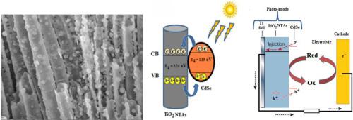
CdSe has attracted interest as the absorber layer in photoelectrochemical cell applications. In this work, titania nanotubes thin film electrodes were prepared by the anodisation method of titanium foil were used due to their ability to produce a uniformly stable structure with high surface area, excellent charge transfer, low interfacial grain boundaries and effective absorption of light. Three electrochemical deposition techniques were used to deposit CdSe onto TiO2 NTAs, namely potentiostatic deposition, cyclic voltammetric deposition, and pulse electrodeposition techniques as a novel to compare between these methods. X-ray diffractometry (XRD), field emission scanning electron microscopy (FESEM) coupled with energy dispersive X-ray spectroscopy (EDX), high-resolution transmission electron microscopy (HRTEM), and UV–Visible diffuse reflectance spectroscopy were used for the characterization of CdSe/TiO2 NTAs nanostructures. The photoelectrochemical performance of the nanostructured CdSe/TiO2 NTAs was investigated in 0.01 M Na2S under visible light illumination. The use of pulse electrodeposition resulted in a greater uniformity in the distribution of CdSe loaded onto TiO2 nanotube arrays. Thus the performance of semiconductor heterostructures prepared by this technique shows a substantial improvement compared to the other two techniques.
中文翻译:
电沉积技术通过均匀分布CdSe纳米粒子敏化TiO 2纳米管阵列光电极
CdSe作为光电化学电池应用中的吸收层引起了人们的兴趣。在这项工作中,使用钛箔的阳极氧化方法制备了二氧化钛纳米管薄膜电极,因为它们能够产生具有高表面积,优异的电荷转移,低界面晶界和有效吸收光的均匀稳定的结构。使用三种电化学沉积技术将CdSe沉积到TiO 2上NTAs,即恒电位沉积,循环伏安沉积和脉冲电沉积技术,是在这些方法之间进行比较的一种新颖方法。X射线衍射法(XRD),场发射扫描电子显微镜(FESEM)结合能量色散X射线光谱法(EDX),高分辨率透射电子显微镜(HRTEM)和紫外可见漫反射光谱法进行了表征CdSe / TiO 2 NTAs纳米结构的制备。在可见光照射下,在0.01 M Na 2 S中研究了纳米结构的CdSe / TiO 2 NTAs的光电化学性能。脉冲电沉积的使用导致负载在TiO 2上的CdSe的分布更加均匀纳米管阵列。因此,与其他两种技术相比,通过这种技术制备的半导体异质结构的性能显示出显着的提高。


 京公网安备 11010802027423号