当前位置:
X-MOL 学术
›
Plasma Processes Polym.
›
论文详情
Our official English website, www.x-mol.net, welcomes your
feedback! (Note: you will need to create a separate account there.)
Hard silicon carbonitride thin‐film coatings produced by remote hydrogen plasma chemical vapor deposition using aminosilane and silazane precursors. 1: Deposition mechanism, chemical structure, and surface morphology
Plasma Processes and Polymers ( IF 2.9 ) Pub Date : 2021-02-15 , DOI: 10.1002/ppap.202000240 Aleksander M. Wrobel 1 , Pawel Uznanski 1
Plasma Processes and Polymers ( IF 2.9 ) Pub Date : 2021-02-15 , DOI: 10.1002/ppap.202000240 Aleksander M. Wrobel 1 , Pawel Uznanski 1
Affiliation
|
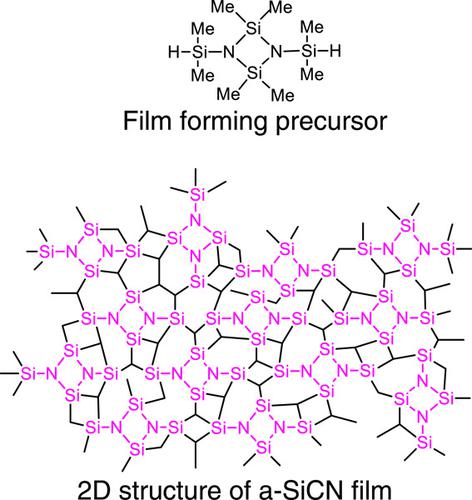
Amorphous silicon carbonitride films were produced by remote hydrogen microwave plasma chemical vapor deposition (RP‐CVD) using aminosilanes: (dimethylamino)dimethylsilane, bis(dimethylamino)methylsilane, and tris(dimethylamino)silane, as well as disilazanes: 1,1,3,3‐tetramethyldisilazane and 1,3‐bis(dimethylsilyl)‐2,2,4,4‐tetramethylcyclodisilazane as single‐source precursors. The effect of substrate temperature (TS) on the rate and yield of the RP‐CVD process, chemical composition, chemical structure, and surface morphology of resulting films is reported. The temperature dependencies of thickness‐based growth rate and growth yield of the film imply that for a low substrate temperature range (TS = 30–200°C), deposition rate and yield are limited by desorption of film‐forming precursors from a growth surface, whereas for a high substrate temperature range (TS = 200–400°C), the rate and yield values, independent of the temperature, are nearly constant and the RP‐CVD is a nonthermally activated process. The increase of the substrate temperature from 30°C to 400°C causes the elimination of organic groups from the film and the formation of a silicon carbonitride network structure with a predominant content of Si–N nitridic and Si–C carbidic bonds. On the basis of structural study and literature data, hypothetical elementary reactions contributing to the film formation process are postulated. The films were found to be morphologically homogeneous, defect‐free materials exhibiting very small surface roughness, which varied in a narrow range of values.
中文翻译:

使用氨基硅烷和硅氮烷前体通过远程氢等离子体化学气相沉积制得的硬质碳氮化硅薄膜涂层。1:沉积机理,化学结构和表面形态
使用氨基硅烷:(二甲基氨基)二甲基硅烷,双(二甲基氨基)甲基硅烷和三(二甲基氨基)硅烷以及二硅氮烷:1,1,3通过远程氢微波等离子体化学气相沉积(RP-CVD)制备非晶碳氮化硅膜,3-三甲基二硅氮烷和1,3-双(二甲基甲硅烷基)-2,2,4,4-四甲基环二硅氮烷作为单一来源的前体。衬底温度的影响(Ť小号报道的速率和RP-CVD工艺的产率,化学组成,化学结构,和得到的薄膜的表面形态)。膜的基于厚度的生长速率和生长速率的温度依赖性表明,对于低基材温度范围(T S = 30-200℃),沉积速率和产率被膜形成前体的解吸从生长表面的限制,而对于高的衬底的温度范围(Ť小号 = 200–400°C),速率和屈服值几乎与温度无关,并且RP-CVD是非热激活过程。基板温度从30°C升高到400°C会导致薄膜中有机基团的消失,并形成主要包含Si-N氮键和Si-C碳键的碳氮化硅网络结构。根据结构研究和文献数据,假定了有助于成膜过程的基本反应。发现这些膜是形态均匀的无缺陷材料,具有非常小的表面粗糙度,其值在狭窄的范围内变化。
更新日期:2021-02-15
中文翻译:
使用氨基硅烷和硅氮烷前体通过远程氢等离子体化学气相沉积制得的硬质碳氮化硅薄膜涂层。1:沉积机理,化学结构和表面形态
使用氨基硅烷:(二甲基氨基)二甲基硅烷,双(二甲基氨基)甲基硅烷和三(二甲基氨基)硅烷以及二硅氮烷:1,1,3通过远程氢微波等离子体化学气相沉积(RP-CVD)制备非晶碳氮化硅膜,3-三甲基二硅氮烷和1,3-双(二甲基甲硅烷基)-2,2,4,4-四甲基环二硅氮烷作为单一来源的前体。衬底温度的影响(Ť小号报道的速率和RP-CVD工艺的产率,化学组成,化学结构,和得到的薄膜的表面形态)。膜的基于厚度的生长速率和生长速率的温度依赖性表明,对于低基材温度范围(T S = 30-200℃),沉积速率和产率被膜形成前体的解吸从生长表面的限制,而对于高的衬底的温度范围(Ť小号 = 200–400°C),速率和屈服值几乎与温度无关,并且RP-CVD是非热激活过程。基板温度从30°C升高到400°C会导致薄膜中有机基团的消失,并形成主要包含Si-N氮键和Si-C碳键的碳氮化硅网络结构。根据结构研究和文献数据,假定了有助于成膜过程的基本反应。发现这些膜是形态均匀的无缺陷材料,具有非常小的表面粗糙度,其值在狭窄的范围内变化。


 京公网安备 11010802027423号