Materials Today Physics ( IF 10.0 ) Pub Date : 2021-02-11 , DOI: 10.1016/j.mtphys.2021.100369 Yancheng Chen , Yingjie Lu , Xun Yang , Shunfang Li , Kaiyong Li , Xuexia Chen , Zhiyang Xu , Jinhao Zang , Chongxin Shan
|
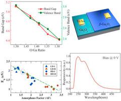
Gallium oxide (Ga2O3) has recently emerged as a promising candidate for applications in high-power and radio frequency electronics, deep-ultraviolet optoelectronics, etc. The engineering of bandgap and constructing of heterostrucutres are fundamental steps towards such applications. However, efficient bandgap engineering of Ga2O3 is still a huge challenge. Herein, by the combination of experiments and first-principles calculations, we report that the oxygen vacancy (VO) density and crystalline disorder of the Ga2O3 can be tuned continuously by modulating the O/Ga ratio during the growth process. The VO can introduce localized defect states right above the valence band, thus improving the conductivity of the films. While the crystalline disorder can lead to the shift of the valence band towards the conduction band, thus narrowing the bandgap of the Ga2O3 significantly. As a demonstration of the practical applications of the bandgap engineering by the crystalline disorder, Ga2O3-based deep-ultraviolet homojunction photodetectors have been developed. The device shows a peak responsivity of 22.1 mA/W and a detectivity of 8.7 × 10¹² Jones at 0 V bias, which are among the best values for zero-biased Ga2O3 photodetectors. The present findings on tuning the bandgap of Ga2O3 via structural disorder are expected to pave a new avenue to achieving high performance Ga2O3 optoelectronic and electronic devices.
中文翻译:
晶体缺陷对氧化镓的带隙工程
氧化镓(Ga 2 O 3)最近已成为在大功率和射频电子,深紫外光电等领域中应用的有希望的候选者。带隙的工程设计和异质结构的构建是实现此类应用的基本步骤。但是,Ga 2 O 3的有效带隙工程仍然是巨大的挑战。在本文中,通过实验和第一性原理计算的结合,我们报道了可以通过在生长过程中调节O / Ga比来连续调节Ga 2 O 3的氧空位(V O)密度和晶体无序性。在V Ô可以在价带正上方引入局部缺陷状态,从而提高薄膜的导电性。尽管结晶无序可能导致价带向导带移动,从而使Ga 2 O 3的带隙显着变窄。为了证明由晶体无序引起的带隙工程的实际应用,已经开发了基于Ga 2 O 3的深紫外同质结光电探测器。该器件在0 V偏压下显示出22.1 mA / W的峰值响应度和8.7×10 12 Jones的检测率,这是零偏压Ga 2 O 3的最佳值光电探测器。当前关于通过结构无序调节Ga 2 O 3 的带隙的发现有望为实现高性能Ga 2 O 3光电和电子设备铺平道路。


 京公网安备 11010802027423号