Microelectronics Journal ( IF 1.9 ) Pub Date : 2021-01-27 , DOI: 10.1016/j.mejo.2021.105001 Bahram Jafari , Javad Tavakoli , Samad Sheikhaei
|
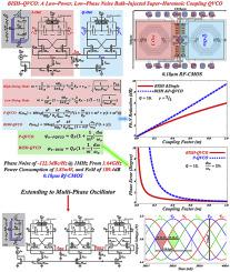
In this paper, a novel method of Super–Harmonic coupling is proposed to generate quadrature outputs. In this method, by direct connection of all switching transistors bulk terminals, a second harmonic current is injected from each one of the I/Q oscillators to the other. Therefore, the proposed circuit is called Body–Injected Super–Harmonic coupling (BISH–) QVCO. The quadrature operation of the proposed circuit is mathematically proven and certified by simulations. In addition, through a detailed analysis, closed–form expressions are derived for the output phase noise and phase error. To have a fair performance evaluation of the proposed topology, the proposed BISH-QVCO, and the conventional P–QVCO are designed and simulated in 0.18 μm RF-CMOS technology with 3.22–3.64 GHz oscillation frequency (12.25% tuning range), a power supply of 1.8V, and the same power consumption of 3.85 mW. The quality factor of the tank circuits is calculated as 9.2. Post layout simulation results predict phase noise of −122.3dBc/Hz at 1 MHz offset from 3.64 GHz oscillation frequency that presents 4.1 dB and 2.7 dB phase noise improvements compared to the conventional P–QVCO and simple LC VCO, respectively. The maximum I and Q outputs phase error due to a 2% tank capacitor mismatch is 7°. A FOMT of 189.4 dB is achieved for the proposed QVCO. Also, the proposed method is capable of generating multi–phase outputs, which can be ranked among the well-performing ones.
中文翻译:
BISH-QVCO:低功率,低噪声,大体积注入的超谐波耦合QVCO
在本文中,提出了一种新的超谐波耦合方法来产生正交输出。在这种方法中,通过所有开关晶体管体端子的直接连接,二次谐波电流从每个I / Q振荡器注入到另一个。因此,拟议的电路称为人体注入超谐波耦合(BISH)QVCO。拟议电路的正交运算已通过数学验证并通过仿真证明。此外,通过详细的分析,可以得出输出相位噪声和相位误差的闭式表达式。为了对提议的拓扑进行公平的性能评估,拟议的BISH-QVCO和常规的P–QVCO在0.18μmRF-CMOS技术中进行了设计和仿真,具有3.22–3.64 GHz的振荡频率(12.25%的调谐范围), 1.8V电源,而相同的功耗为3.85毫瓦。储能回路的品质因数计算为9.2。布局后的仿真结果预测,与3.64 GHz振荡频率相比,在3.64 GHz振荡频率偏移1 MHz时,相位噪声为−122.3dBc / Hz,与传统的P-QVCO和简单的LC VCO相比,相位噪声分别提高了4.1 dB和2.7 dB。由于2%的储能电容失配而导致的最大I和Q输出相位误差为7°。FOM 由于2%的储能电容失配而导致的最大I和Q输出相位误差为7°。FOM 由于2%的储能电容失配而导致的最大I和Q输出相位误差为7°。FOM牛逼的189.4分贝是拟议QVCO实现。此外,所提出的方法能够产生多-相输出,可在良好的执行者可以排。


 京公网安备 11010802027423号