Our official English website, www.x-mol.net, welcomes your
feedback! (Note: you will need to create a separate account there.)
Effects of the thickness and laser irradiation on the electrical properties of e-beam evaporated 2D bismuth
Nanoscale ( IF 5.8 ) Pub Date : 2021-1-2 , DOI: 10.1039/d0nr06062c Xinghao Sun 1, 2, 3, 4, 5 , Hanliu Zhao 1, 2, 3, 4, 5 , Jiayi Chen 1, 2, 3, 4, 5 , Wen Zhong 1, 2, 3, 4, 5 , Beibei Zhu 1, 2, 3, 4, 5 , Li Tao 1, 2, 3, 4, 5
Nanoscale ( IF 5.8 ) Pub Date : 2021-1-2 , DOI: 10.1039/d0nr06062c Xinghao Sun 1, 2, 3, 4, 5 , Hanliu Zhao 1, 2, 3, 4, 5 , Jiayi Chen 1, 2, 3, 4, 5 , Wen Zhong 1, 2, 3, 4, 5 , Beibei Zhu 1, 2, 3, 4, 5 , Li Tao 1, 2, 3, 4, 5
Affiliation
|
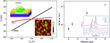
Two-dimensional (2D) bismuth is expected to yield exotic electrical properties for various nanoelectronics, despite the difficulty in large-area preparation and property tuning directly on a device substrate. This work reports electron beam (e-beam) evaporation of large-area 2D bismuth directly on SiO2/Si with an electrical conductivity of ∼105 S m−1 and a field effect carrier mobility of ∼235 cm2 V−1 s−1 at room temperature, comparable to those of the molecular beam epitaxy (MBE) counterparts with a similar thickness. Interestingly, the electrical conductivity of 2D bismuth changes when exposed to laser irradiation that possibly induced an increase of the defect concentration, indicating a potential photo-sensor application. The electrical response of 2D bismuth can be modified either by laser irradiation or by varying the layer thickness. Due to the dimension and surface state effects in 2D bismuth, the layer thickness has a strong influence on the carrier concentration and mobility. Inspiringly, a simultaneous increase of the electrical conductivity and the Seebeck coefficient was achieved in 2D bismuth, which is preferred for thermoelectric performance but rarely reported. Our results provided a more accessible platform than MBE to produce decent quality 2D bismuth and similar Xenes with tunable electrical properties for various nanoelectronics.
中文翻译:

厚度和激光辐照对电子束蒸发二维铋的电学性能的影响
尽管很难进行大面积制备和直接在器件基板上进行性能调整,但二维(2D)铋有望产生各种纳米电子学的特殊电性能。这项工作报告了直接在SiO 2 / Si上大面积二维铋的电子束(电子束)蒸发,电导率约为10 5 S m -1,场效应载流子迁移率约为235 cm 2 V -1 s -1在室温下,与具有相似厚度的分子束外延(MBE)相当。有趣的是,二维铋的电导率在暴露于激光辐照时会发生变化,这可能会导致缺陷浓度的增加,表明潜在的光电传感器应用。二维铋的电响应可以通过激光辐照或通过改变层厚来改变。由于二维铋的尺寸和表面状态效应,层厚度对载流子浓度和迁移率有很大影响。令人鼓舞的是,在二维铋中实现了电导率和塞贝克系数的同时增加,这对于热电性能而言是优选的,但鲜有报道。
更新日期:2021-01-26
中文翻译:
厚度和激光辐照对电子束蒸发二维铋的电学性能的影响
尽管很难进行大面积制备和直接在器件基板上进行性能调整,但二维(2D)铋有望产生各种纳米电子学的特殊电性能。这项工作报告了直接在SiO 2 / Si上大面积二维铋的电子束(电子束)蒸发,电导率约为10 5 S m -1,场效应载流子迁移率约为235 cm 2 V -1 s -1在室温下,与具有相似厚度的分子束外延(MBE)相当。有趣的是,二维铋的电导率在暴露于激光辐照时会发生变化,这可能会导致缺陷浓度的增加,表明潜在的光电传感器应用。二维铋的电响应可以通过激光辐照或通过改变层厚来改变。由于二维铋的尺寸和表面状态效应,层厚度对载流子浓度和迁移率有很大影响。令人鼓舞的是,在二维铋中实现了电导率和塞贝克系数的同时增加,这对于热电性能而言是优选的,但鲜有报道。


 京公网安备 11010802027423号