当前位置:
X-MOL 学术
›
Nanoscale Adv.
›
论文详情
Our official English website, www.x-mol.net, welcomes your feedback! (Note: you will need to create a separate account there.)
Fully in situ Nb/InAs-nanowire Josephson junctions by selective-area growth and shadow evaporation
Nanoscale Advances ( IF 4.7 ) Pub Date : 2021-1-19 , DOI: 10.1039/d0na00999g Pujitha Perla 1, 2 , H Aruni Fonseka 3 , Patrick Zellekens 1, 2 , Russell Deacon 4 , Yisong Han 3 , Jonas Kölzer 1, 2 , Timm Mörstedt 1, 2 , Benjamin Bennemann 1, 2 , Abbas Espiari 1, 2 , Koji Ishibashi 4 , Detlev Grützmacher 1, 2, 5 , Ana M Sanchez 3 , Mihail Ion Lepsa 2, 5 , Thomas Schäpers 1, 2
Nanoscale Advances ( IF 4.7 ) Pub Date : 2021-1-19 , DOI: 10.1039/d0na00999g Pujitha Perla 1, 2 , H Aruni Fonseka 3 , Patrick Zellekens 1, 2 , Russell Deacon 4 , Yisong Han 3 , Jonas Kölzer 1, 2 , Timm Mörstedt 1, 2 , Benjamin Bennemann 1, 2 , Abbas Espiari 1, 2 , Koji Ishibashi 4 , Detlev Grützmacher 1, 2, 5 , Ana M Sanchez 3 , Mihail Ion Lepsa 2, 5 , Thomas Schäpers 1, 2
Affiliation
|
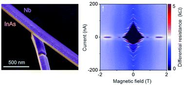
Josephson junctions based on InAs semiconducting nanowires and Nb superconducting electrodes are fabricated in situ by a special shadow evaporation scheme for the superconductor electrode. Compared to other metallic superconductors such as Al, Nb has the advantage of a larger superconducting gap which allows operation at higher temperatures and magnetic fields. Our junctions are fabricated by shadow evaporation of Nb on pairs of InAs nanowires grown selectively on two adjacent tilted Si (111) facets and crossing each other at a small distance. The upper wire relative to the deposition source acts as a shadow mask determining the gap of the superconducting electrodes on the lower nanowire. Electron microscopy measurements show that the fully in situ fabrication method gives a clean InAs/Nb interface. A clear Josephson supercurrent is observed in the current–voltage characteristics, which can be controlled by a bottom gate. The large excess current indicates a high junction transparency. Under microwave radiation, pronounced integer Shapiro steps are observed suggesting a sinusoidal current–phase relation. Owing to the large critical field of Nb, the Josephson supercurrent can be maintained to magnetic fields exceeding 1 T. Our results show that in situ prepared Nb/InAs nanowire contacts are very interesting candidates for superconducting quantum circuits requiring large magnetic fields.
中文翻译:

通过选择性区域生长和阴影蒸发实现全原位 Nb/InAs 纳米线约瑟夫森结
基于 InAs 半导体纳米线和 Nb 超导电极的约瑟夫森结是通过超导电极的特殊阴影蒸发方案原位制造的。与铝等其他金属超导体相比,铌具有较大的超导间隙,可以在更高的温度和磁场下工作。我们的结是通过在两个相邻倾斜的 Si (111) 面上选择性生长并在小距离处相互交叉的 InAs 纳米线对上的 Nb 阴影蒸发制造的。相对于沉积源的上线用作确定下纳米线上的超导电极间隙的荫罩。电子显微镜测量表明,完全原位制造方法提供了干净的 InAs/Nb 界面。在电流-电压特性中观察到明显的约瑟夫森超电流,可以通过底栅控制。大的过电流表示高的结透明度。在微波辐射下,观察到明显的整数夏皮罗阶跃表明正弦电流-相位关系。由于 Nb 的大临界场,约瑟夫森超电流可以维持在超过 1 T 的磁场中。我们的结果表明,原位制备的 Nb/InAs 纳米线触点对于需要大磁场的超导量子电路来说是非常有趣的候选者。
更新日期:2021-01-25
中文翻译:
通过选择性区域生长和阴影蒸发实现全原位 Nb/InAs 纳米线约瑟夫森结
基于 InAs 半导体纳米线和 Nb 超导电极的约瑟夫森结是通过超导电极的特殊阴影蒸发方案原位制造的。与铝等其他金属超导体相比,铌具有较大的超导间隙,可以在更高的温度和磁场下工作。我们的结是通过在两个相邻倾斜的 Si (111) 面上选择性生长并在小距离处相互交叉的 InAs 纳米线对上的 Nb 阴影蒸发制造的。相对于沉积源的上线用作确定下纳米线上的超导电极间隙的荫罩。电子显微镜测量表明,完全原位制造方法提供了干净的 InAs/Nb 界面。在电流-电压特性中观察到明显的约瑟夫森超电流,可以通过底栅控制。大的过电流表示高的结透明度。在微波辐射下,观察到明显的整数夏皮罗阶跃表明正弦电流-相位关系。由于 Nb 的大临界场,约瑟夫森超电流可以维持在超过 1 T 的磁场中。我们的结果表明,原位制备的 Nb/InAs 纳米线触点对于需要大磁场的超导量子电路来说是非常有趣的候选者。


 京公网安备 11010802027423号